Customer CaseElectronics Industry NewsEngineering TechnologiesPCB DesignPCB ManufacturingPCB Materials
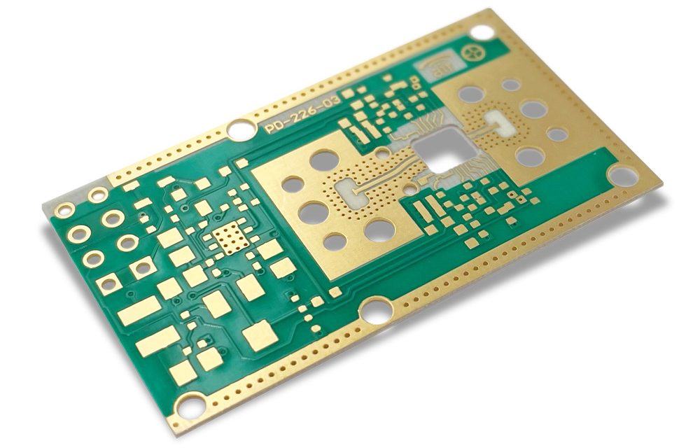
RO4003 PCB for 5G Antenna: Reliable High-Frequency Performance for Advanced Wireless Systems
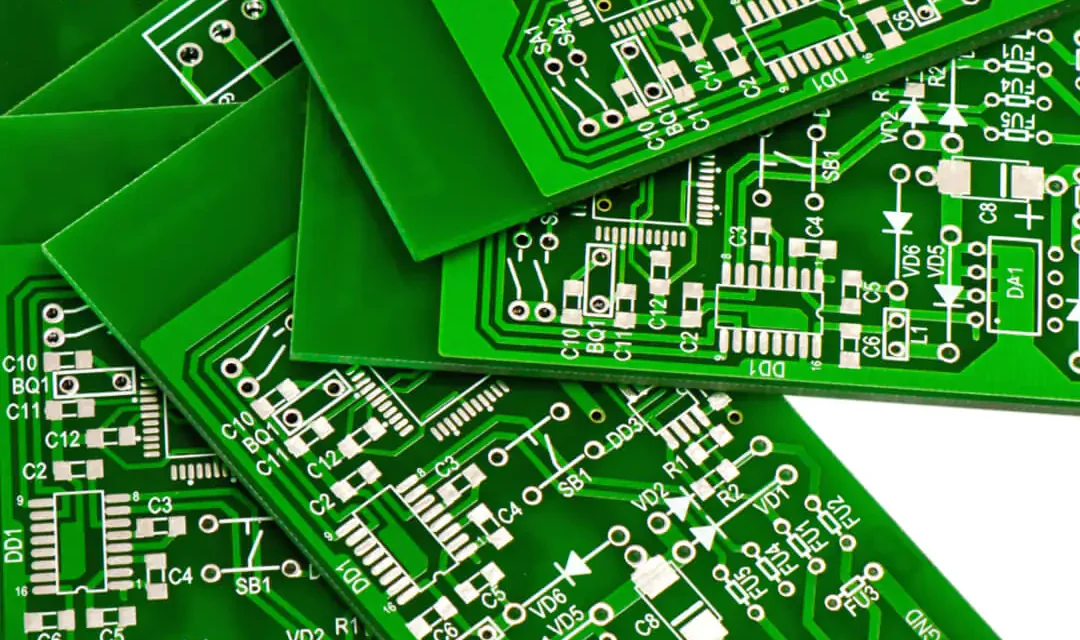
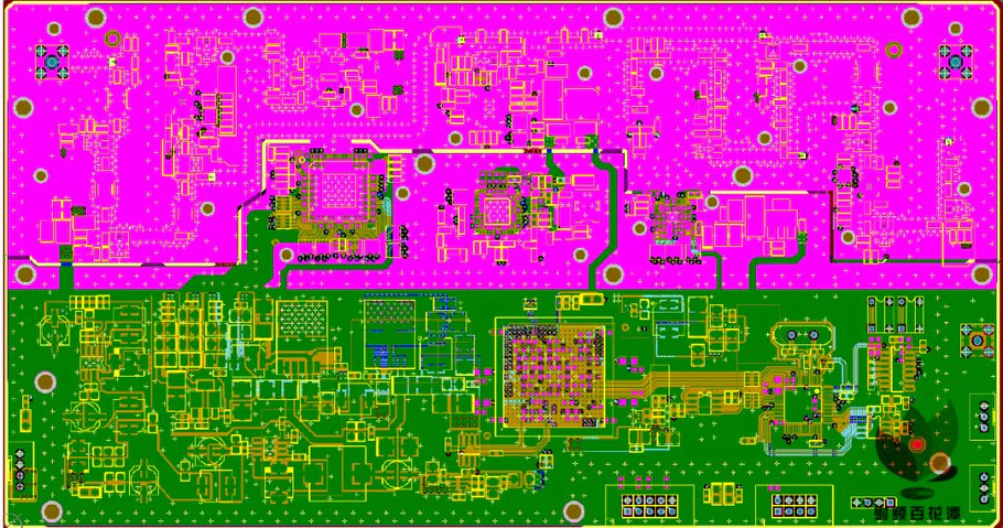
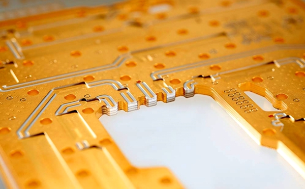
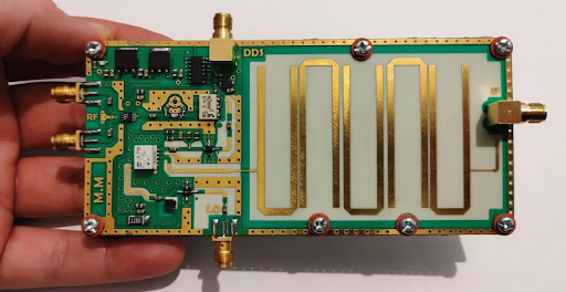
As 5G technology continues to expand across sub-6 GHz and higher frequency bands, antenna performance has become a critical factor in wireless system reliability. The PCB material used for antenna design directly affects signal loss, radiation efficiency, and impedance stability. RO4003 PCB for 5G antenna applications has become a popular choice due to its excellent...