What Is a Signal Integrity PCB?
A Signal Integrity PCB is a printed circuit board specifically designed to preserve the quality, timing, and accuracy of electrical signals as they propagate through high-speed and high-frequency circuits. As signal speeds increase and edge rates become faster, maintaining signal integrity (SI) becomes a critical factor in overall system performance and reliability.
Signal Integrity PCBs are widely used in high-speed digital systems, RF and microwave circuits, 5G communication equipment, data centers, automotive electronics, and semiconductor test boards, where even minor signal distortion can cause system failure.
Why Signal Integrity Matters in Modern PCB Design
Poor signal integrity can lead to multiple performance and reliability issues, including:
-
Signal reflection and ringing
-
Crosstalk between adjacent traces
-
Timing skew and jitter
-
Electromagnetic interference (EMI)
-
Data errors and system instability
A well-designed Signal Integrity PCB ensures clean signal transmission, predictable timing behavior, and stable high-speed operation, especially in dense, multilayer PCB layouts.
Key Design Factors for Signal Integrity PCBs
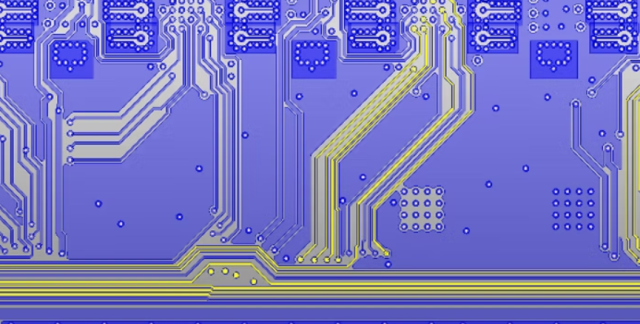
1. Controlled Impedance Routing
Controlled impedance is fundamental to signal integrity. Matching trace impedance to the source and load prevents reflections and ensures consistent signal propagation for high-speed digital and RF signals.
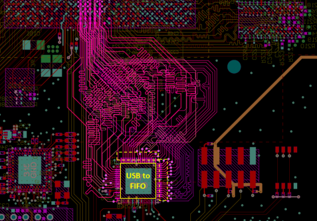
2. Differential Pair Design
High-speed interfaces such as USB, PCIe, Ethernet, and SerDes rely on differential pairs. Proper spacing, length matching, and symmetry are essential to reduce noise and maintain signal integrity.
3. Optimized PCB Stack-Up
An optimized multilayer stack-up with dedicated signal, ground, and power planes provides stable return paths, reduces loop inductance, and minimizes EMI, all of which directly improve signal integrity.
4. Crosstalk Control
High-density routing increases the risk of crosstalk. Signal Integrity PCB designs carefully control trace spacing, routing direction, and layer assignment to minimize coupling between adjacent signals.
5. Low-Loss PCB Materials
Using low dielectric loss laminates helps preserve signal amplitude and reduce attenuation, especially in high-frequency and high-speed applications such as 5G, RF, and microwave systems.
6. Via and Transition Optimization
Poorly designed vias can introduce impedance discontinuities. Signal Integrity PCBs use back-drilling, blind/buried vias, and microvias to minimize signal degradation at layer transitions.
Applications of Signal Integrity PCBs

Signal Integrity PCB solutions are critical in:
-
High-speed computing and server motherboards
-
5G base stations and RF communication modules
-
Automotive ADAS and high-speed ECUs
-
Semiconductor ATE, load boards, and probe cards
-
Networking equipment and data transmission systems
-
IoT and edge computing devices
These applications demand high-speed, low-noise, and highly reliable signal transmission.
KKPCB Signal Integrity PCB Capabilities
KKPCB provides professional Signal Integrity PCB design support and manufacturing services, including:
-
Controlled impedance PCB fabrication
-
High-speed multilayer PCB manufacturing
-
Differential pair routing optimization
-
Low-loss material selection and stack-up design
-
HDI, microvia, and fine-line PCB technology
-
Electrical testing and signal quality verification
Our engineering team focuses on minimizing signal distortion, reducing EMI, and ensuring high-speed reliability throughout the PCB lifecycle.
Conclusion
A Signal Integrity PCB is essential for modern electronic systems operating at high speeds and high frequencies. Through controlled impedance routing, optimized stack-ups, low-loss materials, and advanced via technology, Signal Integrity PCBs ensure accurate, stable, and reliable signal transmission. With advanced manufacturing capabilities and SI-focused engineering expertise, KKPCB delivers high-performance Signal Integrity PCB solutions for demanding applications.
