What Is an Impedance Controlled PCB?
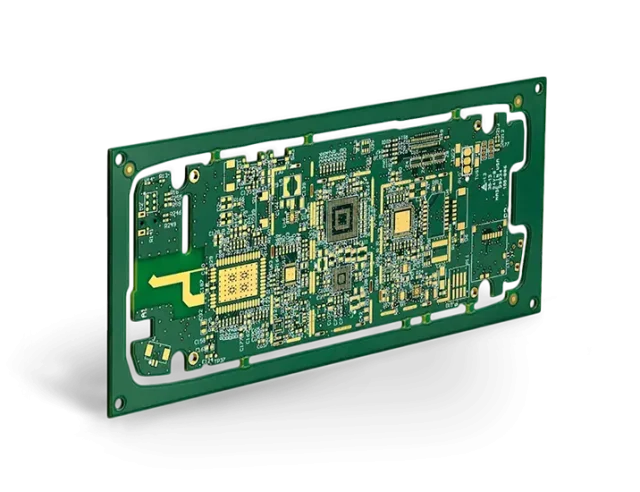
An Impedance Controlled PCB is a printed circuit board designed to maintain precise characteristic impedance along signal traces. This is critical for high speed digital circuits, RF communication, and microwave systems, where mismatched impedance can cause:
-
Signal reflection
-
Crosstalk
-
Data errors
-
Timing skew
Impedance control ensures reliable signal integrity and predictable performance across multiple production batches.
Why Impedance Control Is Important
Modern electronics operate at increasing data rates and frequencies. Without proper impedance control:
-
High speed differential pairs can suffer from reflection and skew
-
RF and microwave signals lose power and accuracy
-
PCB traces may generate electromagnetic interference (EMI)
-
System reliability and test yield decrease
Impedance Controlled PCB is essential in applications such as 5G modules, automotive radar, high speed computing, and IoT sensors.
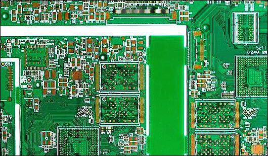
Key Design Features of Impedance Controlled PCB
1. Controlled Trace Width and Spacing
Precise trace width, spacing, and layer stack-up are calculated based on:
-
Desired impedance (50Ω, 75Ω, differential pairs, etc.)
-
Dielectric constant of PCB material (Dk)
-
PCB thickness and copper weight
This ensures consistent signal propagation and minimal reflection.
2. Differential Pair Routing
High speed signals often use differential pairs to:
-
Improve noise immunity
-
Reduce EMI
-
Maintain high data integrity
Length matching and proper spacing are critical for maintaining differential impedance.
3. Low Loss and High Frequency Materials
Materials used in Impedance Controlled PCB must provide:
-
Low dielectric loss (Df)
-
Stable Dk across frequency and temperature
-
Thermal stability for reliable multilayer lamination
Common materials include RO4350B, RO4003C, RF-35, and high TG FR-4.
4. Multilayer and HDI Stack-Ups
Complex designs may require:
-
High layer count (8–20+)
-
Microvia and HDI technology
-
Precise layer alignment
-
Controlled impedance in each signal layer
This supports compact high speed circuits while maintaining signal integrity.
Applications of Impedance Controlled PCB
Impedance Controlled PCB is widely used in:
-
High speed computing boards (CPU/GPU modules)
-
5G communication modules and antennas
-
Automotive radar and LiDAR systems
-
RF front-end modules and test boards
-
Industrial IoT sensor modules
-
High frequency backplanes and network switches
Consistent impedance is critical for minimizing signal loss and maximizing reliability in all these applications.
Impedance Controlled PCB vs Standard PCB
| Feature | Impedance Controlled PCB | Standard PCB |
|---|---|---|
| Signal Integrity | High | Moderate |
| Data Rate Support | GHz / High Speed | Low / Medium |
| Material Requirement | Low loss / Stable Dk | Standard FR-4 |
| Differential Pair Support | Yes | Limited |
| EMI Control | Excellent | Moderate |
For high speed and high frequency applications, impedance controlled PCB is essential.
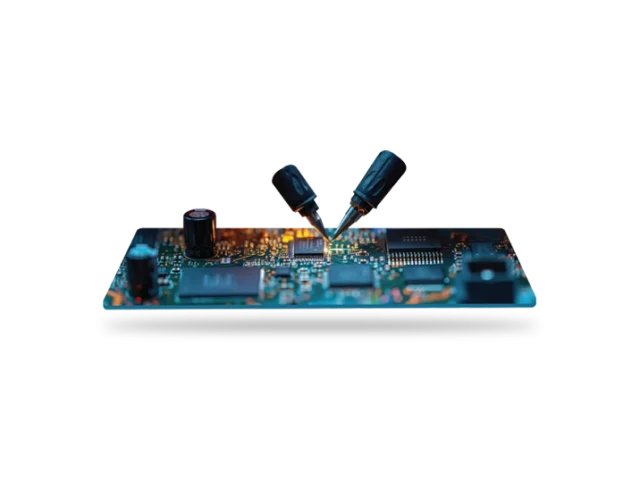
Manufacturing Considerations
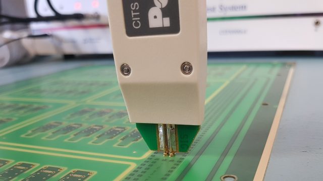
Producing high quality Impedance Controlled PCB requires:
-
Precise material selection
-
Accurate layer stack-up and lamination
-
Trace width and spacing control within tight tolerances
-
Electrical testing for impedance verification
-
Strict quality control and process documentation
Professional PCB manufacturers ensure reliable impedance control and repeatable signal performance.
Conclusion
Impedance Controlled PCB is essential for high speed, high frequency, and RF applications. By ensuring precise impedance, low loss, and high signal integrity, these PCBs enable reliable data transmission in 5G modules, automotive radar, IoT sensors, and high performance computing systems.
Selecting an experienced PCB manufacturer guarantees optimized stack-up design, accurate impedance control, and long-term operational reliability.
