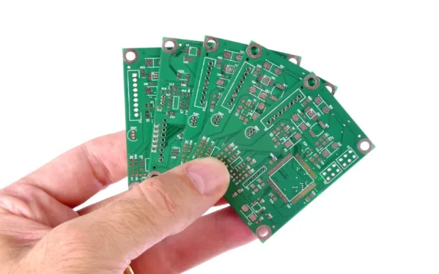
High Speed PCB for Modern Digital Systems

As data rates continue to increase in communication, computing, and semiconductor applications, PCB design must evolve to maintain signal integrity and stable performance. A High Speed PCB is specifically engineered to support high-frequency digital signals, fast edge rates, and high bandwidth transmission.
Unlike standard PCBs, high speed boards require careful control of impedance, layer stack-up, material selection, and routing geometry to prevent signal distortion, reflection, and electromagnetic interference.
High speed PCB design is critical in applications where signal accuracy directly impacts system reliability.
What Defines a High Speed PCB?
A PCB is generally considered “high speed” when:
-
Signal rise/fall times are very fast
-
Data rates exceed hundreds of MHz or multiple GHz
-
Transmission line effects become significant
-
Controlled impedance is required
Common high-speed interfaces include:
-
DDR memory
-
PCIe
-
USB 3.x
-
Ethernet (1G/10G/25G and above)
-
High-speed ADC/DAC systems
At these speeds, PCB layout becomes part of the circuit itself.
Key Design Considerations
1. Controlled Impedance Routing
High speed signals must maintain stable impedance (e.g., 50Ω single-ended, 100Ω differential). This requires:
-
Accurate stack-up design
-
Consistent dielectric thickness
-
Tight trace width tolerance
-
Verified impedance testing
Improper impedance control leads to reflection and signal degradation.
2. Signal Integrity Optimization
Signal integrity challenges include:
-
Crosstalk
-
Reflection
-
Insertion loss
-
Skew between differential pairs
-
Ground bounce
Solutions involve careful spacing, reference plane management, and minimizing discontinuities.
3. Low Loss Materials
As frequency increases, dielectric and conductor losses become significant. High speed PCBs often use:
-
Low Dk and low Df laminates
-
High Tg materials
-
Smooth copper foil for reduced surface roughness
Material choice directly affects insertion loss and signal quality.
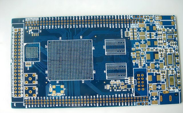
4. Layer Stack-Up Design
Multilayer structures are typically required, including:
-
Dedicated ground planes
-
Power distribution layers
-
Signal layers with controlled reference
-
Proper return path design
An optimized stack-up reduces EMI and ensures stable high-speed transmission.
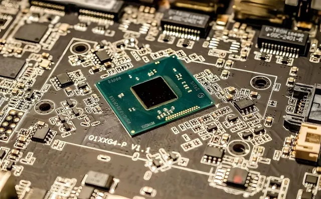
5. Via Optimization
At high frequencies, vias introduce parasitic inductance and capacitance. Techniques such as:
-
Back drilling
-
Blind and buried vias
-
Via stub minimization
help improve high speed performance.
Applications of High Speed PCB
High speed PCBs are widely used in:
-
Data center networking equipment
-
Servers and storage systems
-
5G communication infrastructure
-
Semiconductor test boards
-
AI computing hardware
-
Industrial high-speed control systems
As system bandwidth increases, high speed PCB technology becomes increasingly essential.
High Speed PCB vs Standard PCB
| Feature | Standard PCB | High Speed PCB |
|---|---|---|
| Impedance Control | Optional | Strict |
| Signal Frequency | Low to Moderate | High / GHz |
| Material Requirement | Standard FR4 | Low Loss / High Tg |
| Stack-Up Complexity | Basic | Advanced Multilayer |
| Manufacturing Tolerance | Standard | Tight |
High speed PCB design requires closer collaboration between PCB manufacturer and hardware engineers.
Conclusion
High Speed PCB technology enables reliable signal transmission in modern digital systems operating at increasingly higher data rates. Through precise impedance control, optimized stack-up design, low loss materials, and strict fabrication tolerance, high speed PCBs ensure signal integrity and stable system performance.
As bandwidth demands continue to grow, investing in professional high speed PCB design and manufacturing becomes critical for achieving long-term reliability and performance.
