What Is a Controlled Impedance PCB?
A Controlled Impedance PCB is a printed circuit board engineered to maintain a precise and consistent impedance value along specific signal traces. Impedance control is critical in high speed and high frequency electronic systems where signal integrity directly affects performance and reliability.
In modern electronic designs, signals travel at extremely high speeds. Without proper impedance control, signal reflections, distortion, crosstalk, and electromagnetic interference (EMI) can occur. A Controlled Impedance PCB ensures that signal traces match the target impedance value—commonly 50Ω, 75Ω, 90Ω, or 100Ω differential—through careful stack-up design and manufacturing precision.
Why Controlled Impedance PCB Is Important
1. Prevents Signal Reflection
When trace impedance does not match system impedance, signal reflections occur. This leads to:
-
Data errors
-
Eye diagram degradation
-
Unstable high speed communication
Controlled Impedance PCB minimizes reflection and ensures smooth signal transmission.
2. Ensures Signal Integrity in High Speed Design
High speed interfaces such as:
-
DDR memory
-
PCIe
-
USB
-
HDMI
-
Ethernet
require strict impedance control. Controlled Impedance PCB maintains stable differential pair routing and controlled trace geometry.
3. Supports High Frequency Applications
In RF and microwave systems, impedance control is even more critical. Controlled Impedance PCB enables:
-
Stable RF transmission
-
Reduced insertion loss
-
Predictable electromagnetic behavior
This is essential for 5G communication, radar systems, and RF transceiver modules.
4. Reduces EMI and Crosstalk
Proper impedance matching improves return path continuity and reduces electromagnetic interference. Controlled Impedance PCB is widely used in sensitive industrial and automotive electronics to meet EMC standards.
Key Factors in Controlled Impedance PCB Design
Stack-Up Structure
Accurate layer stack-up planning is the foundation of Controlled Impedance PCB manufacturing. Designers must define:
-
Dielectric thickness
-
Copper weight
-
Reference planes
-
Core and prepreg materials
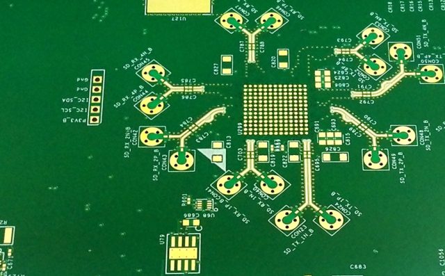
Trace Geometry
Trace width, spacing, and copper thickness directly impact impedance value. Tight tolerance manufacturing is required to maintain accuracy.
Material Selection
Low loss materials and stable dielectric constant (Dk) materials improve impedance consistency, especially in high frequency Controlled Impedance PCB designs.
Manufacturing Tolerance
Precise etching control, lamination pressure, and copper plating uniformity are critical to achieving consistent impedance performance.
Applications of Controlled Impedance PCB
Controlled Impedance PCB is widely used in:
-
High speed server motherboards
-
Data center networking equipment
-
5G telecom infrastructure
-
RF modules and microwave circuits
-
Automotive ADAS systems
-
Industrial automation controllers
-
Aerospace communication systems
These systems require stable signal performance and minimal transmission loss.
Controlled Impedance PCB vs Standard PCB
| Feature | Controlled Impedance PCB | Standard PCB |
|---|---|---|
| Impedance Accuracy | Tight Tolerance | Not Specified |
| Signal Integrity | High | Moderate |
| High Speed Support | Excellent | Limited |
| RF Compatibility | Suitable | Not Optimized |
| Manufacturing Complexity | Higher | Lower |
Controlled Impedance PCB is essential for advanced high speed and high frequency applications.
Conclusion
Controlled Impedance PCB plays a vital role in modern electronics where signal integrity, high speed data transmission, and RF stability are required.
By combining accurate stack-up design, precise trace geometry, and stable material selection, Controlled Impedance PCB ensures reliable performance in demanding communication, computing, and automotive systems.
For high speed digital and RF applications, choosing a professional Controlled Impedance PCB manufacturer ensures consistent quality and predictable electrical performance.
