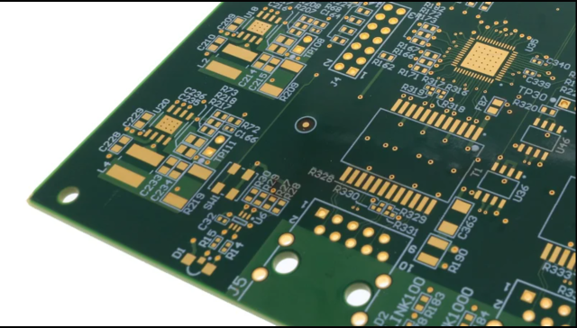
What Is a Fine Line PCB?
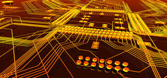
A Fine Line PCB is a printed circuit board designed with ultra-thin traces and narrow spacing, typically under 4 mils (0.1 mm), enabling high-density interconnections for compact electronic devices. Fine line PCBs are essential in applications where space constraints, high-speed signals, and precise routing are required, such as 5G modules, IoT devices, RF circuits, and high-speed computing.
By enabling precise routing, low crosstalk, and consistent impedance, fine line PCBs ensure signal integrity, stable power delivery, and reliable performance in advanced electronic systems.
Why Fine Line PCBs Matter
Fine line PCBs address critical challenges in modern electronics:
-
Miniaturization: fitting more circuitry in smaller areas
-
High-speed signal transmission: maintaining signal fidelity on narrow traces
-
Crosstalk reduction: minimizing interference between adjacent traces
-
Reliability: precise manufacturing prevents shorts and signal degradation
Applications include 5G communications, high-speed logic boards, RF/mixed-signal modules, automotive electronics, IoT devices, and aerospace systems.
Key Design Considerations for Fine Line PCBs
1. Ultra-Thin Trace and Spacing Control
Maintaining trace widths and spacing below 4 mils requires advanced fabrication technology to prevent shorts, impedance mismatch, and signal distortion.
2. Controlled Impedance
High-speed signals and differential pairs require precise impedance control to maintain signal integrity and reduce reflections and ringing.
3. Multilayer Stack-Up Optimization
Fine line PCBs often use multilayer stack-ups with dedicated power and ground planes, minimizing noise and EMI while supporting high-density routing.
4. Low-Loss Materials
Selecting low-loss laminates reduces dielectric loss and preserves high-frequency signals, critical for RF, 5G, and high-speed digital applications.
5. Thermal and Power Management
High-density traces carry higher current density. Proper thermal vias, copper pours, and heat-spreading layers ensure stable performance and long-term reliability.
6. Precision Manufacturing
Fine line PCBs require high-precision etching, advanced inspection, and strict process control to ensure repeatable quality, whether for prototyping or mass production.
Applications of Fine Line PCBs
-
5G RF front-end modules
-
High-speed computing and server motherboards
-
IoT devices and compact wearables
-
Automotive ECUs and ADAS systems
-
RF and mixed-signal modules in aerospace
-
High-density, high-performance electronic devices
KKPCB Fine Line PCB Capabilities
KKPCB provides professional Fine Line PCB design and manufacturing services, including:
-
Trace widths and spacing down to 3–4 mils
-
Controlled impedance and differential pair routing
-
Multilayer HDI PCB fabrication
-
Low-loss material selection for high-frequency applications
-
Thermal and power management optimization
-
Small batch prototyping to large-scale production
Our engineering team ensures every Fine Line PCB meets strict electrical, thermal, and mechanical requirements, delivering high-performance, high-density, and reliable electronic solutions.
Conclusion
A Fine Line PCB is vital for modern high-density and high-speed electronics, ensuring signal integrity, controlled impedance, and reliable operation. By combining precise trace control, optimized multilayer stack-ups, low-loss materials, and advanced manufacturing, KKPCB delivers professional Fine Line PCB solutions for 5G, IoT, automotive, aerospace, and high-speed computing applications.
