
The solder mask, also known as solder resist, is one of the most important layers in a printed circuit board (PCB). Although it is only a thin protective coating, it plays a critical role in PCB reliability, assembly quality, and long-term performance.
A solder mask is the colored insulating layer applied over the copper traces of a PCB, leaving only specific areas exposed for soldering, such as:
- Component pads
- Test points
- Connector contacts
During PCB assembly, the solder mask helps control solder flow, prevent short circuits, and protect the copper surface from environmental damage.
A properly designed solder mask contributes to:
- Improved soldering reliability
- Reduced manufacturing defects
- Better electrical insulation
- Enhanced PCB durability
1. What Is PCB Solder Mask?
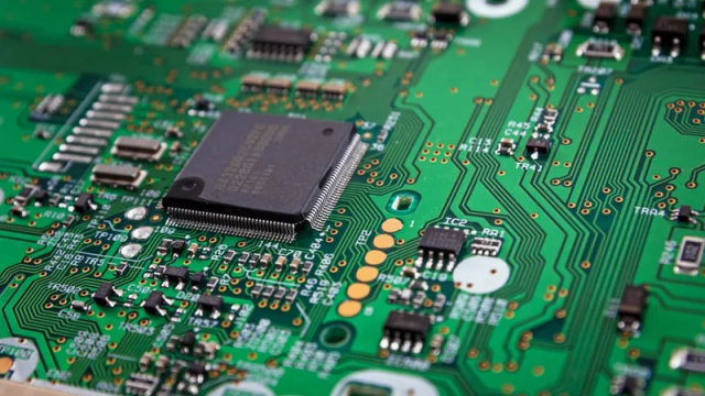
A PCB solder mask is a thin polymer coating applied to the outer copper layers of a circuit board.
Its primary purpose is to protect copper conductors while allowing solderable areas to remain exposed.
A typical PCB structure includes:
Component Layer
       ↓
Silkscreen
       ↓
Solder Mask
       ↓
Copper Layer
       ↓
Dielectric Material
       ↓
Copper Layer
       ↓
Solder Mask
       ↓
Silkscreen
The solder mask is normally applied on:
- Top copper layer
- Bottom copper layer
For multilayer PCBs, it protects the external copper layers.
2. Main Functions of PCB Solder Mask
2.1 Prevents Solder Bridges
During SMT assembly, solder paste is applied to component pads and melted during reflow.
Without solder mask:
- Excess solder may spread between adjacent pads.
- Short circuits may occur.
The solder mask creates insulation between copper features and helps control solder placement.
This is especially important for:
- Fine-pitch IC packages
- QFP components
- BGA packages
- HDI PCBs
2.2 Protects Copper Traces
Copper is vulnerable to:
- Oxidation
- Moisture
- Chemical contamination
The solder mask provides a protective barrier that improves:
- Corrosion resistance
- Electrical stability
- Product lifetime
2.3 Improves PCB Insulation
The solder mask provides electrical separation between conductive areas.
It helps maintain:
- Surface insulation resistance
- Clearance between conductors
- High-voltage reliability
This is particularly important for:
- Power electronics
- Industrial control boards
- Automotive electronics
2.4 Improves Assembly Efficiency
During SMT assembly, the solder mask helps define:
- Solder paste deposition area
- Component placement region
- Solder joint formation
This improves:
- Production yield
- Assembly consistency
- Inspection accuracy
3. Types of PCB Solder Mask
3.1 Liquid Photoimageable Solder Mask (LPI)
LPI solder mask is the most commonly used technology in modern PCB manufacturing.
Process:
- Apply liquid solder mask ink.
- Dry the coating.
- Expose using UV imaging.
- Develop the exposed pattern.
- Cure the solder mask.
Advantages:
- High resolution
- Suitable for fine-pitch components
- Good adhesion
- Wide application range
Used for:
- Multilayer PCBs
- HDI PCBs
- High-density electronic products
3.2 Dry Film Solder Mask
Dry film solder mask uses a photosensitive film laminated onto the PCB surface.
Advantages:
- Good thickness uniformity
- Precise pattern control
Applications:
- High-density PCB manufacturing
- Advanced PCB processes
3.3 Epoxy Liquid Solder Mask
This is a traditional solder mask technology.
Advantages:
- Low cost
- Simple processing
Disadvantages:
- Lower resolution compared with LPI
Commonly used for:
- Simple PCB designs
- Low-cost electronic products
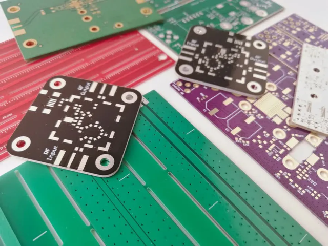
4. Common PCB Solder Mask Colors
Green Solder Mask
The most common PCB color.
Advantages:
- Good contrast during inspection
- Mature manufacturing process
- Cost-effective
Black Solder Mask
Advantages:
- Premium appearance
- Suitable for consumer electronics
Considerations:
- Lower contrast during visual inspection
Blue Solder Mask
Often used for:
- Industrial products
- Development boards
Red Solder Mask
Common in:
- Prototype boards
- Special applications
White Solder Mask
Often used for:
- LED PCBs
because it improves light reflection.
5. PCB Solder Mask Manufacturing Process
Step 1: Surface Preparation
Before solder mask application, the PCB surface is cleaned to remove:
- Oxides
- Dust
- Contaminants
This improves:
- Adhesion
- Coating quality
Step 2: Solder Mask Coating
The solder mask material is applied using methods such as:
- Screen printing
- Curtain coating
- Spray coating
Step 3: Pre-Curing
The coating is partially dried to stabilize the material before imaging.
Step 4: UV Exposure
A photomask defines areas where solder mask should remain or be removed.
Step 5: Development
Unwanted solder mask areas are removed, exposing:
- Component pads
- Test points
Step 6: Final Curing
The solder mask is fully hardened through thermal curing.
This improves:
- Mechanical strength
- Chemical resistance
- Reliability
6. PCB Solder Mask Design Considerations
6.1 Solder Mask Expansion
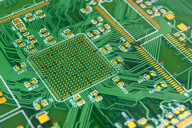
Solder mask openings are usually slightly larger than copper pads.
This difference is called:
Solder mask expansion
It compensates for manufacturing alignment tolerance.
If expansion is too large:
- Reduced insulation distance
- Increased solder bridging risk
If expansion is too small:
- Pads may become partially covered
- Poor solder joints may occur
6.2 Solder Mask Thickness
Typical solder mask thickness:
- Around 10–30 μm
Thickness depends on:
- PCB requirements
- Application environment
- Voltage requirements
For high-voltage applications, thickness and spacing must be carefully controlled.
6.3 Solder Mask Defined (SMD) vs Non-Solder Mask Defined (NSMD)
Solder Mask Defined (SMD)
The solder mask overlaps the edge of the pad.
Advantages:
- Better mechanical support
- Useful for some BGA applications
Non-Solder Mask Defined (NSMD)
The copper pad defines the solder area.
Advantages:
- Better solder joint formation
- Common for fine-pitch components
Used widely in:
- SMT assembly
- BGA packages
6.4 Via Covering and Via Plugging
For advanced PCB designs, vias may need solder mask protection.
Options include:
Tented Via
Solder mask covers the via opening.
Advantages:
- Prevents solder leakage
- Reduces contamination
Via Plugging
Via holes are filled with resin.
Advantages:
- Suitable for HDI PCB
- Improves reliability
Applications:
- BGA escape routing
- High-density PCB designs
7. Solder Mask Challenges in PCB Manufacturing
7.1 Poor Adhesion
Possible causes:
- Surface contamination
- Incorrect curing
- Improper preparation
Results:
- Peeling
- Reduced protection
7.2 Solder Mask Misalignment
Caused by:
- Imaging errors
- Material expansion
- Manufacturing tolerance
Effects:
- Pad coverage
- Assembly defects
7.3 Solder Mask Cracking
Possible causes:
- Mechanical stress
- Thermal cycling
- Excessive thickness
Applications affected:
- Automotive electronics
- Outdoor equipment
- High-temperature systems
7.4 Insufficient Insulation Protection
In high-voltage PCB applications, improper solder mask design may contribute to:
- Leakage current
- Electrical breakdown risks
Design must consider:
- Creepage distance
- Clearance distance
- Operating voltage
8. Solder Mask Selection for Different PCB Applications
| Application | Recommended Consideration |
|---|---|
| Consumer electronics | Standard LPI solder mask |
| Industrial control PCB | High reliability solder mask |
| Automotive PCB | Thermal and chemical resistance |
| RF PCB | Low-loss compatible materials and precise processing |
| HDI PCB | Fine-resolution solder mask |
| Power electronics | Insulation performance and thickness control |
| LED PCB | Reflective white solder mask |
9. Solder Mask and PCB Assembly Reliability
A well-designed solder mask improves:
SMT Assembly Quality
By controlling:
- Solder paste distribution
- Pad separation
- Component alignment
BGA Reliability
By improving:
- Solder joint consistency
- Insulation between pads
Long-Term Product Reliability
By protecting:
- Copper traces
- Conductive paths
- Electrical insulation structures
10. PCB Solder Mask in High-Reliability Applications
For demanding applications such as:
- Industrial automation
- Medical electronics
- Aerospace electronics
- Automotive systems
- Power electronics
solder mask selection should consider:
- Temperature resistance
- Chemical resistance
- Moisture resistance
- Electrical insulation performance
- Manufacturing consistency
Additional protection methods may include:
- Conformal coating
- Encapsulation
- Environmental sealing
Conclusion
PCB solder mask is much more than a protective color coating. It is a critical functional layer that directly affects:
- Electrical insulation
- Assembly quality
- Manufacturing yield
- Product reliability
A properly designed solder mask helps prevent solder bridges, protects copper circuits, improves PCB durability, and supports reliable operation in demanding environments.
For modern PCB applications involving HDI, high-density SMT assembly, industrial control, RF systems, and power electronics, careful solder mask design is an essential part of achieving high-quality and reliable PCB production.
