What Is a Signal Integrity PCB?
A Signal Integrity PCB is a printed circuit board specifically designed and manufactured to ensure high-speed signals remain stable, clean, and reliable from transmitter to receiver. In modern electronics, as data rates increase and edge rates become faster, signal integrity (SI) becomes one of the most critical performance factors in PCB design.
A well-designed Signal Integrity PCB helps reduce signal reflection, impedance discontinuity, crosstalk, EMI noise, jitter, and insertion loss, ensuring consistent performance in high-speed digital, RF, and mixed-signal systems.
Signal Integrity PCBs are widely used in 5G communication, high-speed networking, automotive electronics, industrial control, aerospace systems, and IC test boards where stable signal transmission is essential.
Why Signal Integrity Matters in High-Speed PCB Design
In high-speed circuits, the PCB is no longer a simple interconnect. Every trace becomes a transmission line, and every via, connector, pad, and plane transition can impact performance. Poor signal integrity may lead to:
-
Unstable communication and data errors
-
Increased bit error rate (BER)
-
Timing margin reduction and jitter problems
-
EMI compliance failures
-
System instability and random resets
-
Performance degradation at high frequency
That is why Signal Integrity PCB design is essential for reliable, high-speed electronic products.
Key Features of a Signal Integrity PCB
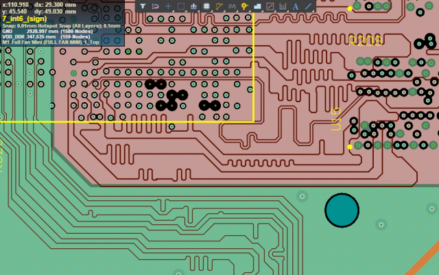
1. Controlled Impedance PCB Design
A high-quality Signal Integrity PCB requires accurate controlled impedance, especially for:
-
Microstrip transmission lines
-
Stripline transmission lines
-
High-speed differential pair PCB routing
Maintaining stable impedance (such as 50Ω single-ended or 90Ω/100Ω differential) reduces reflections and ensures consistent signal quality.
2. Differential Pair Routing for Signal Integrity
Many high-speed interfaces depend on differential pair PCB routing, including USB, PCIe, HDMI, LVDS, and high-speed SerDes. A Signal Integrity PCB ensures:
-
Consistent differential impedance
-
Tight pair-to-pair length matching
-
Stable spacing and coupling control
-
Smooth via transitions and minimized stubs
Proper differential routing improves noise immunity and EMI performance, helping the system pass high-speed signal compliance requirements.
3. Low Crosstalk and Noise Control
Crosstalk is a major issue in dense high-speed routing. A Signal Integrity PCB minimizes crosstalk by using:
-
Proper trace spacing and isolation
-
Ground shielding and reference planes
-
Correct layer assignment in multilayer PCB stack-up
-
Controlled return current paths
Reducing crosstalk improves overall signal integrity and prevents random signal interference.
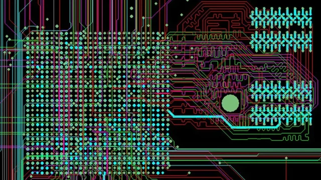
4. Optimized PCB Stack-Up for Signal Integrity
A professional Signal Integrity PCB stack-up is the foundation of stable performance. A well-designed stack-up improves:
-
Signal return path continuity
-
Plane capacitance for noise suppression
-
EMI containment and shielding
-
Impedance consistency across layers
Multilayer stack-ups also help separate high-speed signals from sensitive analog or power circuits, improving overall reliability.
5. Via Design and Stub Control
Vias can create impedance discontinuities and cause reflections, especially at high-speed and high-frequency. A Signal Integrity PCB often includes:
-
Backdrill vias to remove stubs
-
Optimized via-to-plane clearance
-
Reduced via count in critical paths
-
Proper via placement for return current continuity
High-speed PCB via optimization is a key factor for stable signal integrity.
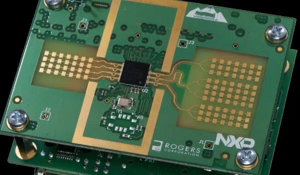
6. Low Loss PCB Materials for High-Speed Signals
For high data rate applications, FR-4 may introduce too much loss. A Signal Integrity PCB may use low loss PCB materials such as:
-
Megtron series laminates
-
Rogers high-frequency materials
-
Low Df / low loss prepreg systems
Low loss PCB materials reduce insertion loss and maintain signal quality across long trace lengths and high-frequency operation.
Common Applications of Signal Integrity PCB
Signal Integrity PCBs are essential in many advanced electronic systems, including:
-
High-speed networking equipment (switches, routers, servers)
-
5G communication systems (base stations, RF modules)
-
Automotive electronics (ADAS, radar, ECU high-speed links)
-
Aerospace and defense electronics (high-reliability high-speed boards)
-
IC test PCB and ATE boards (high-speed signal validation)
-
Industrial automation and control systems
-
Medical electronics requiring stable high-speed communication
KKPCB Signal Integrity PCB Manufacturing Capabilities
KKPCB provides professional Signal Integrity PCB manufacturing with engineering support to meet strict high-speed requirements. Our capabilities include:
-
Controlled impedance PCB fabrication with tight tolerance
-
High-speed differential pair PCB support
-
Multilayer PCB stack-up optimization
-
Fine line PCB and high-density routing for SI-critical designs
-
Backdrill and via stub control options
-
Low loss PCB material sourcing and processing
-
Signal integrity-focused DFM review to improve yield and reliability
-
Prototype to mass production for high-speed PCB projects
We help customers achieve better signal integrity by combining design experience, stable PCB processes, and strict inspection standards.
Best Practices to Improve Signal Integrity PCB Performance
To achieve better signal integrity, consider these key recommendations:
-
Choose a proper stack-up with solid reference planes
-
Keep high-speed traces short and avoid unnecessary layer changes
-
Maintain consistent controlled impedance
-
Use differential pair routing rules strictly
-
Minimize via count and optimize via transitions
-
Ensure a clean return current path and avoid plane splits
-
Use low loss PCB materials when frequency/data rate is high
-
Separate noisy circuits from sensitive signal integrity paths
A professional Signal Integrity PCB strategy helps reduce risk and ensures stable performance in high-speed electronics.
Conclusion
A Signal Integrity PCB is critical for modern high-speed electronics, ensuring stable data transmission with minimal noise, reflection, and crosstalk. With controlled impedance design, optimized stack-up, low loss materials, and precision manufacturing, Signal Integrity PCBs enable reliable performance in 5G, networking, automotive, aerospace, and IC test applications.
KKPCB supports customers with high-quality Signal Integrity PCB manufacturing, delivering stable performance, high reliability, and consistent production quality for signal integrity critical designs.
