What Is a Power Integrity PCB?
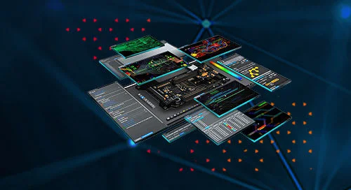
A Power Integrity PCB (PI PCB) is designed to maintain stable voltage, low noise, and reliable power delivery across high-speed circuits and high-density electronic systems. In modern electronics, where switching speeds are faster and current densities higher, power integrity is crucial to avoid voltage drops, ground bounce, and signal errors.
Power Integrity PCBs are widely applied in 5G communication modules, high-speed computing, automotive electronics, IoT devices, and industrial systems, ensuring that sensitive circuits receive consistent and clean power.
Why Power Integrity Matters
Without proper power integrity:
-
Voltage drops and IR drops can compromise performance
-
Ground bounce may cause timing errors
-
Electromagnetic interference (EMI) can increase
-
High-speed circuits may suffer reliability issues
A properly designed Power Integrity PCB ensures stable voltage, low noise, and optimal operation, which is critical for multilayer, high-speed, and high-density PCB designs.
Key Design Considerations for Power Integrity PCBs
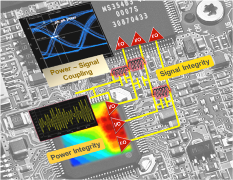
1. Optimized Power Delivery Network (PDN)
A robust PDN includes dedicated power and ground planes, reducing impedance and voltage fluctuations, and supporting high-speed ICs and RF circuits.
2. Decoupling and Bypass Capacitors
Strategically placed capacitors near ICs stabilize local voltages and minimize high-frequency noise, maintaining both signal integrity and power stability.
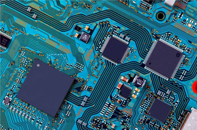
3. Low Impedance and Heavy Copper Layers
Thicker copper layers reduce resistance, support higher currents, and minimize voltage drops, ensuring reliable operation under high loads.
4. Multilayer Stack-Up Optimization
Separating signal, power, and ground planes helps maintain consistent voltage levels, low noise, and reduced EMI across multilayer designs.
5. Thermal Management
High-current or high-density circuits generate heat. Thermal vias, heat-spreading planes, and optimized copper allocation ensure temperature stability and long-term reliability.
6. Material Selection
Low-loss, high-Tg PCB laminates help reduce dielectric loss and voltage ripple, essential for high-speed, high-performance electronics.
Applications of Power Integrity PCBs
-
High-speed computing and server motherboards
-
5G RF modules and communication devices
-
Automotive ECUs and ADAS electronics
-
Industrial automation and motor drives
-
IoT devices with high-speed processors
-
Semiconductor testing and ATE systems
KKPCB Power Integrity PCB Capabilities
KKPCB offers complete Power Integrity PCB solutions, including:
-
Multilayer PCB fabrication with optimized PDN
-
Controlled impedance and low-loss material selection
-
High-current and high-density PCB design
-
Thermal management and mechanical reinforcement
-
Small batch prototyping and full-scale production
-
Electrical verification and quality assurance
Our engineers ensure every Power Integrity PCB meets strict electrical, thermal, and reliability requirements for industrial, automotive, and high-performance electronics.
Conclusion
A Power Integrity PCB is essential for high-speed, high-density electronic systems, ensuring stable voltage, low noise, and reliable performance. By combining optimized PDN, decoupling strategies, low-impedance copper layers, thermal management, and high-quality materials, KKPCB delivers professional Power Integrity PCB solutions that meet the demands of modern electronics.
