In today’s rapidly evolving electronics market, devices are becoming smaller, faster, and more complex. To meet these demands, Microvia PCBs have become a critical solution in HDI PCB and high-speed PCB design. Microvias are extremely small vias that create precise interlayer connections, allowing for high-density routing, improved signal integrity, and reliable performance in modern electronic devices.
What is a Microvia PCB?
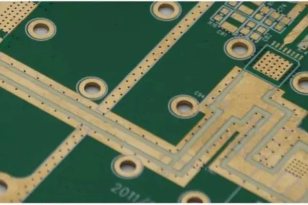
A Microvia PCB is a high-density printed circuit board that uses microvias—typically ≤150 microns in diameter—to connect multiple layers of a board without taking up significant space. This makes Microvia PCBs ideal for HDI PCB applications where compact size and high functionality are essential.
Microvias can be classified into three main types:
-
Blind Vias: Connect outer layers to internal layers without going through the entire board.
-
Buried Vias: Connect internal layers only, hidden from the surface.
-
Stacked/Sequential Microvias: Multi-level microvias for complex multi-layer high-speed PCB designs.
Advantages of Microvia PCBs in HDI and High-Speed Applications
-
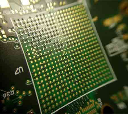
High-Density Routing
Microvias enable finer line widths and smaller spacing, increasing routing density on HDI PCBs and allowing more functionality in compact designs. -
Improved Signal Integrity
Shorter interlayer connections reduce parasitic capacitance and inductance, enhancing performance in high-speed PCB applications. -
Compact and Lightweight Designs
Critical for smartphones, tablets, wearables, and IoT devices where space and weight are limited. -
Multi-Layer PCB Support
Blind and buried microvias allow designers to create complex multi-layer HDI PCB layouts without enlarging board size. -
Enhanced Reliability
Microvia PCBs provide robust mechanical strength and consistent performance, ideal for high-speed and mission-critical electronics.
Manufacturing Process of Microvia PCBs
Producing a high-quality Microvia PCB requires precise manufacturing techniques:
-
Laser Drilling
Laser drilling allows precise, small, and consistent microvias with smooth walls, essential for HDI PCB integrity. -
Copper Plating
Copper is plated inside the microvias to ensure excellent electrical conductivity and mechanical strength for high-speed PCB applications. -
Lamination & Pressing
Multi-layer HDI boards are pressed under heat, forming a stable structure with precise layer alignment. -
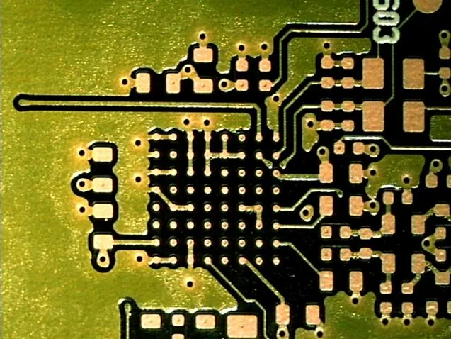
Patterning and Etching
Advanced photolithography creates fine lines and pads, supporting high-density routing and high-speed PCB performance. -
Surface Finishing
ENIG (Electroless Nickel Immersion Gold) or HASL (Hot Air Solder Leveling) finishes protect the PCB and ensure solderability. -
Rigorous Quality Control
Automated Optical Inspection (AOI), X-ray inspection, and electrical testing ensure microvias are defect-free and meet reliability standards.
Applications of Microvia PCBs
Microvia PCBs are widely used where space, speed, and reliability are critical:
-
Smartphones & Tablets: Enabling compact, feature-rich devices.
-
High-Performance Computing: Reliable high-speed signal transmission in servers and data centers.
-
Wearables & IoT Devices: Lightweight, small, and durable electronics.
-
Automotive Electronics: ADAS systems and intelligent control modules needing robust, high-speed connections.
-
Medical Devices: High-density, reliable PCBs for compact diagnostic and monitoring equipment.
Future Trends in Microvia PCB Technology
-
Smaller and Denser Microvias: Further reducing via size for increased routing density.
-
Advanced Materials: Using low-loss laminates for high-frequency high-speed PCB applications.
-
Precision Manufacturing: Enhanced laser drilling, plating, and lamination techniques for improved HDI PCB reliability.
-
Flexible HDI & Microvia Integration: Combining flexibility and high-density routing for wearable and IoT electronics.
Conclusion
Microvia PCBs are essential for HDI PCB and high-speed PCB applications. Their ability to provide high-density routing, superior signal integrity, and reliable multi-layer connections makes them ideal for modern electronics—from smartphones to automotive systems and high-performance computing devices. Partnering with a skilled Microvia PCB manufacturer ensures your products achieve peak performance, reliability, and design efficiency.
