As electronic systems continue to deliver higher bandwidth, faster data rates, and more compact designs, PCB material selection becomes a key factor in achieving stable and reliable performance. In high-speed digital systems and high-frequency applications, traditional FR-4 materials may cause excessive signal loss, impedance instability, and increased crosstalk, especially when signals operate at multi-GHz frequencies.
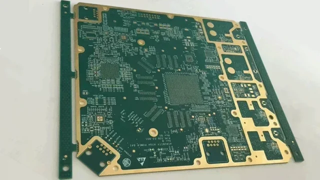
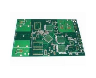
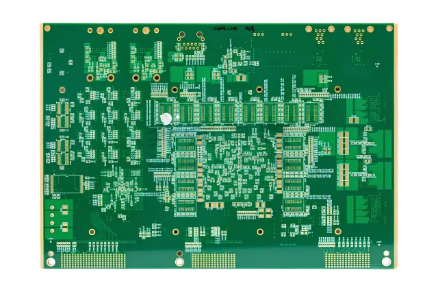
Megtron PCB is widely recognized as a high-performance, low-loss PCB material family designed to support high-speed signal transmission, excellent signal integrity, and stable controlled impedance. Megtron laminates are commonly used in advanced electronics such as servers, networking equipment, data center hardware, 5G infrastructure, and high-speed communication systems where performance and reliability are critical.
This article explains what Megtron PCB is, why it is used, and what design and manufacturing considerations matter most for Megtron PCB projects.
What Is a Megtron PCB?

A Megtron PCB is a printed circuit board manufactured using Panasonic Megtron laminate materials, which are engineered for low dielectric loss and stable electrical performance at high frequencies. Megtron PCB materials are designed for applications that require:
-
Low insertion loss for high-speed channels
-
Stable dielectric constant (Dk) for impedance control
-
Reliable performance for multilayer and high-layer-count PCBs
-
Improved signal integrity for high-speed digital routing
-
Strong thermal and mechanical reliability in advanced assemblies
Compared to standard FR-4, Megtron PCB provides better performance for high-speed logic, high-frequency signals, and complex multilayer stack-ups.
Why Megtron PCB Is Used for High-Speed and High-Frequency Designs
1. Low Loss Performance for High-Speed Signal Transmission
In high-speed digital systems, insertion loss can limit channel length and reduce overall performance. Megtron PCB materials are designed to reduce dielectric loss, helping maintain signal amplitude and eye diagram quality.
Megtron PCB low-loss performance supports:
-
Higher data rates and longer trace routing
-
Improved margin for high-speed interfaces
-
Reduced attenuation for high-frequency signal paths
-
Better reliability in backplanes and long channels
For data center and networking applications, Megtron PCB is often selected to meet strict loss budgets.
2. Excellent Signal Integrity and Reduced Crosstalk
Signal integrity becomes more challenging as edge rates increase and routing density grows. Megtron PCB helps improve signal integrity by reducing loss and supporting consistent impedance behavior across traces.
Key signal integrity benefits include:
-
Cleaner waveforms and reduced jitter
-
Lower crosstalk between high-speed differential pairs
-
Improved return loss and reduced reflections
-
More stable performance across frequency ranges
Megtron PCB is widely used for high-speed logic PCB designs where maintaining signal integrity is critical.
3. Stable Controlled Impedance for High-Speed Digital and RF Routing
Controlled impedance is essential for modern electronics, including:
-
High-speed differential pair PCB routing
-
High-speed serial links and connectors
-
RF and microwave routing in communication systems
Megtron PCB materials provide stable dielectric properties that support accurate impedance targets such as 50Ω single-ended and 100Ω differential.
With proper stack-up design, Megtron PCB enables predictable controlled impedance and consistent production results.
Common Applications of Megtron PCB
Megtron PCB is used across industries that require low-loss and high-performance PCB solutions, including:
-
Servers and data center hardware
-
Networking switches and routers
-
High-speed backplane PCB and interconnect systems
-
5G base stations and communication infrastructure
-
High-speed digital computing platforms
-
High-frequency signal transmission systems
-
Industrial communication and automation equipment
-
Aerospace and defense electronics requiring high reliability
Megtron PCB is a strong choice when both performance and reliability are required in high-speed environments.
Megtron PCB vs Standard FR-4 PCB
Many high-speed designs begin with FR-4, but performance limitations appear as frequency and data rate increase.
FR-4 Challenges in High-Speed Designs
-
Higher dielectric loss at GHz frequencies
-
Reduced channel length due to insertion loss
-
More impedance variation across manufacturing batches
-
Increased risk of crosstalk and EMI issues
Megtron PCB Advantages
-
Lower insertion loss for high-speed channels
-
Better signal integrity and reduced attenuation
-
Stable Dk and impedance behavior
-
Improved performance for multilayer and high layer count PCBs
For demanding high-speed systems, Megtron PCB provides better electrical performance and higher design margin.
Megtron PCB Stack-Up Design Considerations
Stack-up design directly affects signal integrity and impedance control. A well-optimized Megtron PCB stack-up helps achieve:
-
Controlled impedance routing for differential pairs and single-ended traces
-
Stable return paths and reference planes
-
Reduced EMI and improved power distribution
-
Better layer-to-layer consistency for high-speed channels
Megtron PCB stack-ups often include multiple signal layers and reference planes to support high-speed routing and minimize noise coupling.
Megtron PCB Manufacturing Considerations
To ensure stable performance, Megtron PCB fabrication requires precise control of key processes:
1. Trace Geometry and Etching Accuracy
High-speed impedance depends on trace width and spacing. Tight etching control ensures consistent impedance results.
2. Lamination and Dielectric Thickness Control
Stack-up accuracy is critical for impedance stability. Controlled lamination ensures consistent dielectric thickness across panels.
3. Via Quality and Reliability
High-speed signals often transition between layers. Reliable drilling and plating improve via performance and reduce discontinuities.
4. Controlled Impedance Testing
For many Megtron PCB projects, impedance testing is required to confirm performance targets.
5. High Layer Count and Advanced PCB Builds
Megtron PCB is often used in high-layer-count PCBs, where manufacturing capability and process control directly impact yield and reliability.
Best Practices for Designing a Megtron PCB
To achieve the best results in Megtron PCB projects, engineers should follow proven design guidelines:
-
Define target impedance early and confirm with stack-up calculations
-
Use continuous reference planes for stable return paths
-
Keep differential pairs tightly coupled and length-matched
-
Minimize stubs and optimize via transitions
-
Reduce crosstalk with proper spacing and routing rules
-
Use back-drilling when required for high-speed connectors
-
Validate signal integrity through simulation when necessary
These practices help maximize Megtron PCB performance in high-speed and high-frequency designs.
Conclusion: Megtron PCB for Low-Loss High-Speed Electronics
Megtron PCB is a high-performance, low-loss PCB material family designed to support high-speed digital systems, controlled impedance routing, and excellent signal integrity. It is widely used in servers, networking equipment, data centers, and advanced communication infrastructure such as 5G systems.
With proper stack-up design and professional fabrication control, Megtron PCB enables stable high-speed signal transmission and reliable performance in complex multilayer designs.
If you are looking for Megtron PCB fabrication, controlled impedance manufacturing, or high-speed multilayer PCB production, KKPCB can support your project from engineering review to mass production.
