A Low Loss PCB is a specialized printed circuit board designed to minimize signal attenuation, dielectric loss, and insertion loss in high-speed digital and high-frequency RF applications. As modern electronics operate at multi-GHz frequencies and multi-gigabit data rates, signal loss caused by PCB materials and structures becomes a critical limiting factor.
Low loss PCBs are widely used in 5G communication systems, RF and microwave modules, high-speed computing, automotive radar, and semiconductor test PCBs, where signal integrity and measurement accuracy are essential.
Why Low Loss Matters in Modern PCB Design
At high frequencies, signal degradation is no longer dominated by resistance alone. Dielectric loss (Df), conductor loss, and surface roughness all contribute to performance limitations. A low loss PCB addresses these challenges by:
-
Reducing dielectric loss tangent (Df)
-
Maintaining stable dielectric constant (Dk)
-
Optimizing trace geometry and surface finish
-
Ensuring controlled impedance consistency
This results in cleaner eye diagrams, lower jitter, and improved RF performance.
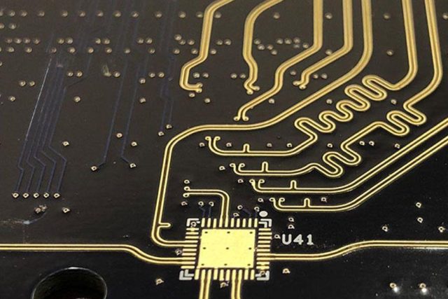
Key Design Features of Low Loss PCBs
1. Low Dk / Low Df Materials
Low loss PCBs typically use advanced materials with low dielectric constant and low dissipation factor, enabling stable signal transmission at high frequencies and reducing insertion loss.
2. Controlled Impedance Routing
Precise impedance control is essential for high-speed and RF signals. Low loss PCB designs incorporate tight trace width tolerance, optimized stackups, and accurate reference planes.
3. Optimized Multilayer Stackups
Dedicated signal, power, and ground layers help reduce crosstalk, EMI, and return path discontinuities, improving overall signal integrity.
4. Low-Parasitic Via Structures
Blind vias, buried vias, and microvias are often used to shorten signal paths and minimize parasitic inductance, which is critical in low loss PCB design.
5. Surface Roughness Control
Smooth copper foil and appropriate surface treatments help reduce conductor loss, especially at high frequencies where skin effect dominates.
Advantages of Low Loss PCBs
-
Reduced insertion loss and signal attenuation
-
Improved signal integrity at high data rates
-
Stable performance across wide frequency ranges
-
Lower jitter and noise for digital signals
-
Accurate RF and microwave signal transmission
These advantages make low loss PCBs essential for next-generation communication and test systems.
Applications of Low Loss PCBs
Low loss PCBs are commonly used in:
-
High-speed IC test PCBs and ATE load boards
-
5G base stations and mmWave modules
-
RF and microwave communication systems
-
Automotive radar and ADAS electronics
-
Data center, networking, and high-speed computing
-
Semiconductor characterization and validation boards
In all these applications, PCB signal loss directly impacts system performance and test accuracy.
Manufacturing Requirements for Low Loss PCBs
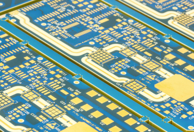
Producing reliable low loss PCBs requires:
-
Precise impedance and thickness control
-
Advanced multilayer lamination and registration
-
High-quality copper foil and surface finish selection
-
Strict process control to ensure consistency
-
Electrical testing and impedance verification
An experienced manufacturer ensures repeatable electrical performance, high yield, and reliable long-term stability.
Conclusion
A Low Loss PCB is a critical foundation for high-speed digital, RF, and high-frequency electronic systems. By combining low Dk/Df materials, controlled impedance routing, optimized multilayer structures, and advanced via technology, low loss PCBs deliver superior signal integrity, reduced attenuation, and reliable performance.
Choosing a professional low loss PCB manufacturer ensures accurate signal transmission, consistent quality, and efficient support from prototype development to mass production.
