What Is a High Speed PCB?
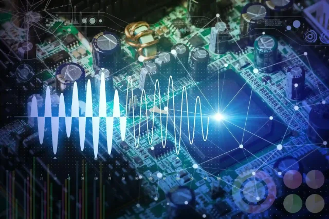
A High Speed PCB is a printed circuit board specifically designed to support high data rate digital signals. As signal edge rates become faster and transmission speeds reach multi-gigabit levels, PCB layout and stack-up design directly affect signal integrity.
High-speed PCB design focuses on maintaining clean signal transmission while minimizing reflection, crosstalk, and electromagnetic interference.
When Does a PCB Become “High Speed”?
A PCB is considered high speed when:
-
Signal rise/fall times are very fast
-
Data rates exceed 1 Gbps
-
Differential signaling is used
-
Trace lengths approach electrical wavelength
-
Controlled impedance becomes mandatory
In modern systems such as DDR memory, PCIe, USB 3.x, and high-speed Ethernet, PCB design plays a critical role in performance stability.
Key Design Principles of High Speed PCB
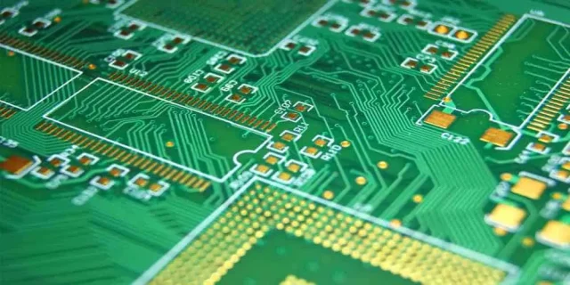
1. Controlled Impedance Routing
High-speed signals must travel through precisely calculated transmission lines.
Common impedance targets:
-
50Ω single-ended
-
100Ω differential
-
85Ω differential (USB)
Stack-up and trace geometry must be tightly controlled.
2. Signal Integrity Optimization
Important considerations include:
-
Reflection control
-
Crosstalk reduction
-
Return path continuity
-
Via stub minimization
-
Length matching for differential pairs
Improper layout may cause eye diagram degradation and data errors.
3. Low-Loss Materials
At high data rates, dielectric loss becomes significant.
Low Dk and low Df materials help:
-
Reduce insertion loss
-
Maintain signal amplitude
-
Improve long-distance routing performance
Material selection directly impacts channel budget.
4. Power Integrity Design
Stable power delivery is critical for high-speed ICs.
Design techniques include:
-
Dedicated power planes
-
Decoupling capacitor optimization
-
Short return paths
-
Plane-to-plane coupling
Noise on power rails can directly affect signal jitter.
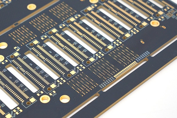
5. Advanced Via Structures
To reduce signal degradation, high-speed PCBs often use:
-
Back-drilled vias
-
Microvias
-
Blind and buried vias
These structures reduce stub length and signal reflection.
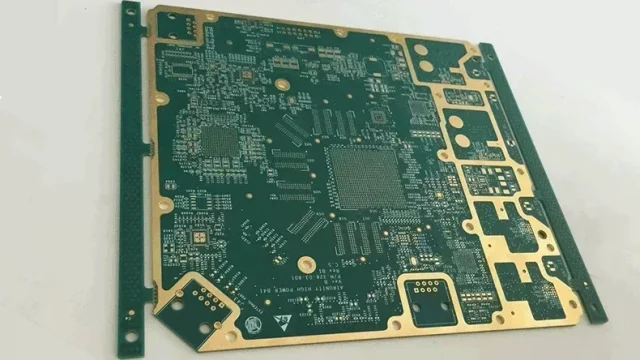
High Speed PCB vs Standard PCB
| Feature | Standard PCB | High Speed PCB |
|---|---|---|
| Impedance Control | Optional | Mandatory |
| Material Selection | General FR4 | Low-loss materials preferred |
| Length Matching | Basic | Precise |
| Crosstalk Control | Limited | Critical |
| Signal Integrity Analysis | Rare | Required |
High-speed PCB design requires simulation and engineering validation.
Applications of High Speed PCB
High Speed PCBs are widely used in:
-
Data center servers
-
AI accelerator boards
-
High-performance computing systems
-
Networking switches and routers
-
5G communication equipment
-
Automotive ADAS platforms
-
Industrial automation systems
As data throughput increases, high-speed PCB design becomes essential.
Conclusion
High Speed PCB technology ensures stable signal transmission in modern high data rate electronic systems. Through controlled impedance routing, low-loss materials, optimized stack-up, and signal integrity engineering, it supports reliable multi-gigabit communication.
For advanced computing, networking, and communication platforms, High Speed PCB design is a foundational requirement for performance and reliability.
