What Is a High Speed Logic PCB?
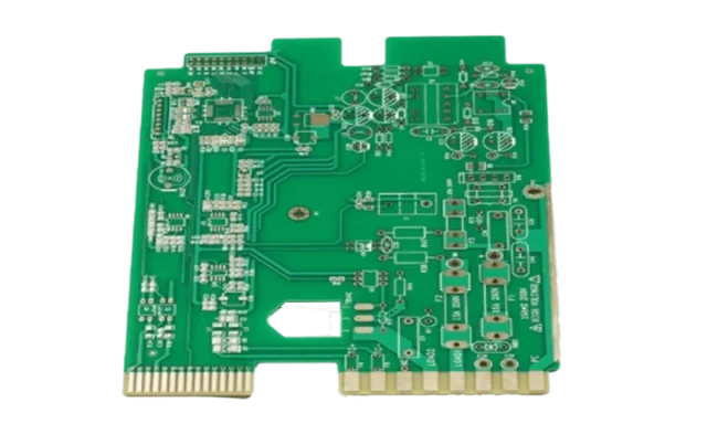
A High Speed Logic PCB is a printed circuit board designed for high-speed digital logic signals that require stable timing, clean waveforms, and reliable data transmission. Unlike standard PCBs, a High Speed Logic PCB must handle fast edge rates, high-frequency harmonics, and strict signal integrity requirements for interfaces such as DDR memory, PCIe, Ethernet, USB, SerDes, FPGA/CPU high-speed buses, and other advanced digital systems.
High Speed Logic PCB design focuses on reducing signal reflection, crosstalk, EMI noise, jitter, insertion loss, and timing skew, ensuring stable operation for high-speed logic circuits in complex electronic products.
Why High Speed Logic PCB Design Matters
As logic devices become faster and more integrated, the PCB plays a major role in overall performance. Poor High Speed Logic PCB design may lead to:
-
Data transmission errors and unstable communication
-
Timing failures and reduced eye opening
-
Increased jitter and skew between signals
-
EMI problems and compliance risks
-
Random system crashes and reliability issues
-
Higher debugging cost and longer development cycles
That is why High Speed Logic PCB layout and manufacturing require controlled impedance, optimized stack-up, and strict process control.
Key Features of a High Speed Logic PCB
1. Controlled Impedance PCB for High-Speed Signals
A High Speed Logic PCB typically requires controlled impedance routing to maintain consistent signal transmission. Common impedance targets include:
-
50Ω single-ended impedance
-
90Ω / 100Ω differential impedance
Controlled impedance helps reduce reflections, improves waveform quality, and supports stable high-speed performance.
2. High-Speed Differential Pair Routing
Many high-speed logic interfaces depend on differential pairs. A High Speed Logic PCB must support:
-
Consistent differential impedance
-
Tight length matching and delay control
-
Stable spacing and coupling
-
Symmetrical routing and smooth transitions
Differential pair routing improves noise immunity and reduces EMI, making it essential for High Speed Logic PCB applications.
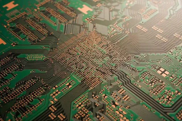
3. Multilayer Stack-Up Optimization
A professional multilayer PCB stack-up is critical for High Speed Logic PCB performance. Proper stack-up design provides:
-
Solid reference planes for return current paths
-
Better EMI shielding and noise control
-
Stable impedance control across layers
-
Improved power integrity with power/ground plane coupling
High Speed Logic PCBs often use 6-layer, 8-layer, 10-layer, or higher layer count to support dense routing and high-speed logic requirements.
4. Signal Integrity PCB Practices
A High Speed Logic PCB is strongly connected to signal integrity PCB design. Key SI practices include:
-
Short and direct routing for critical nets
-
Avoiding stubs and unnecessary vias
-
Maintaining continuous reference planes
-
Minimizing impedance discontinuities
-
Using proper termination where needed
Strong signal integrity ensures stable high-speed logic operation under real-world conditions.
5. Power Integrity Support for Logic ICs
High-speed logic devices such as CPUs and FPGAs require stable power rails. A High Speed Logic PCB should include:
-
Low impedance PDN design
-
Proper decoupling capacitor placement
-
Clean power and ground planes
-
Reduced ground bounce and switching noise
Good power integrity improves timing stability and reduces jitter in high-speed logic systems.
6. EMI and Crosstalk Control
High-speed logic circuits generate high-frequency noise. A High Speed Logic PCB reduces EMI and crosstalk through:
-
Layer-based routing strategy (stripline routing for sensitive nets)
-
Adequate spacing between high-speed signals
-
Ground stitching vias and shielding structures
-
Proper return path control and plane continuity
This helps improve EMC performance and prevents interference between logic signals.
7. Via Design and High-Speed Transitions
Vias can introduce discontinuities that affect signal integrity. High Speed Logic PCB via design often includes:
-
Reduced via count on critical nets
-
Optimized via pad and antipad design
-
Via stitching for stable reference return
-
Backdrill options for removing via stubs (if required)
Optimized via transitions improve eye diagram performance and reduce reflection issues.
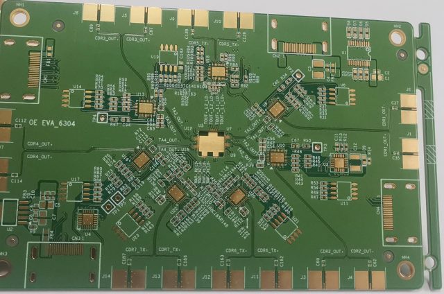
Common Applications of High Speed Logic PCB
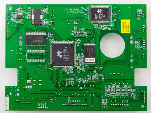
High Speed Logic PCBs are widely used in advanced electronics such as:
-
FPGA and CPU control boards
-
DDR memory interface PCBs
-
PCIe and high-speed SerDes backplanes
-
High-speed networking equipment (switches, routers, servers)
-
Industrial automation and control systems
-
Automotive computing and ADAS electronics
-
Aerospace and defense digital systems
-
IC test PCB and ATE high-speed logic boards
KKPCB High Speed Logic PCB Manufacturing Capabilities
KKPCB provides professional High Speed Logic PCB solutions with engineering support from prototype to mass production, including:
-
Controlled impedance PCB manufacturing
-
Multilayer PCB stack-up design support
-
High-density PCB and fine line PCB fabrication
-
HDI PCB and microvia options for advanced routing
-
Low loss PCB materials for high-speed performance
-
High reliability testing and inspection
-
Signal integrity and power integrity focused DFM review
With stable production processes and strict quality control, KKPCB ensures every High Speed Logic PCB meets the requirements of high-speed digital performance, reliability, and manufacturability.
Conclusion
A High Speed Logic PCB is essential for modern high-speed digital systems, ensuring stable timing, clean signals, and reliable high-speed communication. By combining controlled impedance routing, multilayer stack-up optimization, signal integrity practices, power integrity support, and EMI control, High Speed Logic PCBs deliver consistent performance in demanding applications such as networking, computing, automotive, and IC testing.
KKPCB provides high-quality High Speed Logic PCB manufacturing to support next-generation high-speed electronics with reliable performance and stable production quality.
