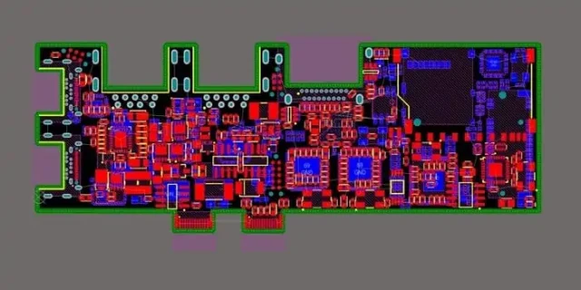
What Is a Fine Line PCB?

A Fine Line PCB is a printed circuit board designed with ultra-narrow traces and spacing, typically below 100 µm. This allows for high-density component placement, complex routing, and miniaturized PCB designs. Fine line PCBs are essential in high-speed digital, RF, 5G, IoT, and aerospace electronics, where both signal integrity and board compactness are critical.
Why Fine Line PCB Design Is Important
As electronic devices become smaller and faster, conventional PCB trace widths and spacing cannot support high-speed or high-density circuits. Fine line PCBs enable:
-
Smaller PCB footprints without sacrificing functionality
-
High-speed signal transmission with minimal reflections
-
Reduced crosstalk between closely spaced traces
-
Compatibility with fine-pitch components such as BGA, QFP, and chip-scale packages
Key Design Considerations
-
Ultra-Fine Trace and Spacing
-
Trace widths down to 50–75 µm or less
-
Laser imaging and high-resolution photolithography ensure precision
-
-
Controlled Impedance
-
Maintains consistent signal speed for high-speed digital and RF signals
-
Critical for differential pairs and high-frequency traces
-
-
Optimized Multilayer Stack-Up
-
Dedicated power and ground planes reduce noise and EMI
-
Supports high-density routing with minimal signal interference
-
-
Material Selection
-
Low-loss laminates with high Tg for high-frequency reliability
-
Compatible with fine-pitch assembly processes
-
-
Thermal Management
-
Prevents overheating in dense layouts with high-speed or high-current traces
-
Applications of Fine Line PCBs
-
5G communication modules and RF front-end boards
-
High-speed computing and data processing systems
-
IoT and wearable electronics
-
Aerospace and defense high-density PCBs
-
Advanced automotive electronics and ADAS systems
KKPCB Fine Line PCB Capabilities
KKPCB provides professional fine line PCB manufacturing and assembly, including:
-
Multilayer PCB fabrication with ultra-fine traces
-
Controlled impedance for high-speed digital and RF circuits
-
HDI PCB and fine-pitch component support
-
Small batch prototyping and large volume production
-
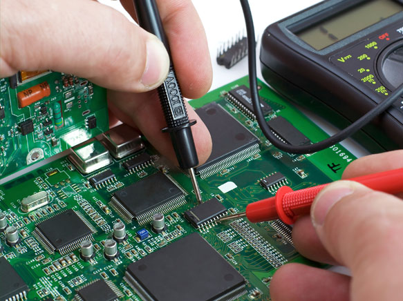
Quality assurance and electrical testing for high reliability
Conclusion
Fine Line PCBs are critical for modern electronics requiring high-density routing, precise signal integrity, and compact design. By combining advanced design, controlled impedance, and multilayer manufacturing, KKPCB delivers **high-performance, reliable fine line
