What Is a Blind Via PCB?
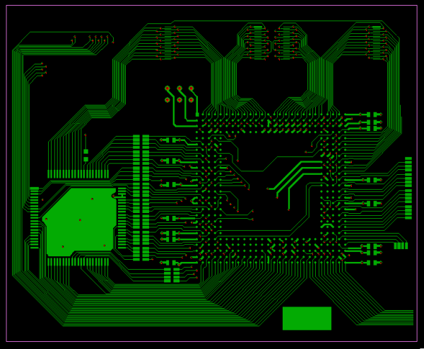
A Blind Via PCB is a type of printed circuit board that contains vias connecting internal layers to one or more outer layers without passing completely through the board. Unlike through-hole vias, blind vias help:
-
Reduce board size
-
Increase routing density
-
Optimize multilayer stack-ups
-
Support HDI (High Density Interconnect) designs
Blind Via PCB is widely used in smartphones, 5G modules, automotive electronics, IoT sensors, and high speed computing boards.
Advantages of Blind Via PCB
1. Higher Routing Density
Blind vias allow designers to connect inner signal layers directly to outer layers, freeing up space for:
-
More signal traces
-
Denser component placement
-
Compact module designs
This is especially important for small form factor electronics.
2. Improved Signal Integrity
Blind Via PCB supports:
-
Shorter signal paths
-
Reduced parasitic capacitance and inductance
-
Controlled impedance
-
Better high frequency performance
This ensures reliable high speed digital and RF performance.
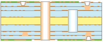
3. Multi-Layer Stack-Up Flexibility
Blind vias are ideal for 8–20+ layer PCBs and HDI designs, allowing:
-
Buried signal routing inside inner layers
-
Hybrid stack-ups combining HDI + standard layers
-
Compact, lightweight boards for portable or automotive electronics
4. Cost and Manufacturing Considerations
While Blind Via PCB can reduce board size and improve performance, it requires:
-
Laser drilling for microvias
-
Precise copper plating and layer alignment
-
Strict lamination control
-
Experienced HDI PCB manufacturers
Proper fabrication ensures reliability and consistent production yield.
Applications of Blind Via PCB
Blind Via PCB is widely used in:
-
High-end smartphones and tablets
-
5G communication modules
-
Automotive radar and ADAS modules
-
Wearable IoT devices
-
High speed computing boards and network switches
-
RF and microwave modules
Blind via technology enables compact design and high density routing without compromising signal integrity.
Blind Via PCB vs Buried and Through-Hole PCB
| Feature | Blind Via PCB | Buried Via PCB | Through-Hole PCB |
|---|---|---|---|
| Connection | Inner layer to outer layer | Inner to inner layer | Through entire board |
| Routing Density | High | Moderate | Limited |
| Signal Path Length | Short | Short | Long |
| Manufacturing Complexity | Moderate-High | High | Low |
| Cost | Moderate | Higher | Low |
Blind vias strike a balance between routing density, signal integrity, and manufacturing cost.
Conclusion
Blind Via PCB is a critical technology for HDI, high layer count, and high speed PCB designs. By connecting internal layers to outer layers without going through the board, it allows compact, high density, and high performance PCBs for smartphones, automotive radar, IoT modules, and 5G applications.
Working with an experienced PCB manufacturer ensures proper laser drilling, plating, lamination, and reliable production yield for blind via technology.
