Why RF Transceiver PCB Technology Is Critical
Modern wireless communication systems are rapidly evolving toward:
- Higher transmission speeds
- Greater communication bandwidth
- Lower latency connectivity
- Compact RF module integration
- Intelligent wireless networking
Applications such as:
- 5G communication systems
- Satellite communication equipment
- IoT wireless devices
- Automotive radar systems
- Aerospace RF electronics
all depend heavily on reliable RF Transceiver PCB technology.
RF transceiver modules are responsible for:
- RF signal transmission
- Wireless signal reception
- Frequency conversion
- Signal amplification
- Communication processing
As operating frequencies continue increasing, PCB design becomes increasingly sensitive to:
- Signal attenuation
- RF interference
- Crosstalk noise
- Thermal instability
- Impedance discontinuities
To achieve stable wireless communication performance, advanced RF Transceiver PCB solutions are essential.
At KKPCB, advanced RF PCB solutions are engineered for:
- High-frequency wireless communication systems
- RF front-end modules
- Microwave multilayer PCB applications
What Is an RF Transceiver PCB?
An RF Transceiver PCB is a high-frequency printed circuit board specifically designed for:
- RF signal transmission and reception
- Wireless communication systems
- Microwave signal processing
- High-speed RF networking platforms
RF transceiver PCB systems commonly integrate:
- RF amplifiers
- RF filters
- Antenna interfaces
- Power management circuits
- High-speed digital communication modules
These PCB systems must provide:
- Stable RF transmission
- Low signal loss
- Excellent signal integrity
- Reliable electromagnetic compatibility
Key Characteristics of RF Transceiver PCB
Low-Loss RF Signal Transmission
RF communication systems require:
- Minimal insertion loss
- Stable microwave transmission
- Reduced signal attenuation
Low-loss RF PCB design improves:
- Wireless communication range
- Signal quality
- Transmission efficiency
This is especially important for:
- 5G wireless infrastructure
- Satellite RF communication
- Automotive radar systems
Excellent Signal Integrity
High-frequency RF systems are extremely sensitive to:
- Signal reflection
- Crosstalk interference
- Electromagnetic noise
- Transmission discontinuities
RF Transceiver PCB design focuses on:
- Controlled routing structures
- Ground plane continuity
- RF isolation optimization
- Differential signal management
These techniques improve:
- Communication reliability
- Data transmission stability
- RF system efficiency
Controlled Impedance Routing
Controlled impedance is essential for:
- RF signal consistency
- Antenna matching
- High-speed communication interfaces
- Microwave transmission stability
RF transceiver PCB routing must carefully optimize:
- Trace geometry
- Dielectric thickness
- Layer stack-up structures
- Return current paths
At KKPCB, advanced multilayer PCB engineering ensures:
- Stable RF transmission performance
- Accurate impedance consistency
- Reliable wireless communication quality
Compact High-Density Integration
Modern RF transceiver systems require:
- Compact PCB architectures
- Miniaturized RF modules
- High-density signal routing
- Integrated antenna structures
HDI PCB technology supports:
- Fine-pitch RF packaging
- Compact multilayer integration
- High-speed signal routing capability
These technologies improve:
- System miniaturization
- RF communication efficiency
- Wireless module integration density
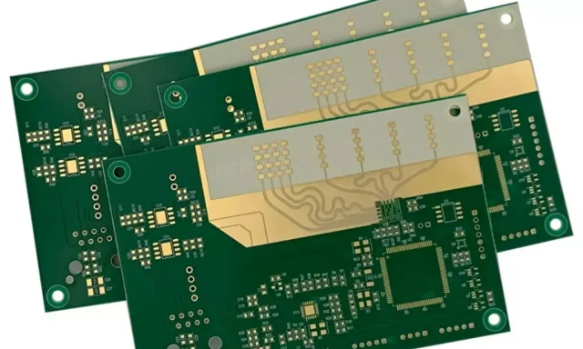
PCB Materials for RF Transceiver PCB
Material selection strongly affects:
- RF transmission quality
- Signal integrity
- Thermal stability
- High-frequency electrical performance
Common RF PCB materials include:
- Rogers RF laminates
- PTFE-based materials
- Hydrocarbon ceramic laminates
- Low-loss high-speed PCB materials
Important material properties include:
- Low dielectric loss
- Stable dielectric constant
- Excellent thermal reliability
- High-frequency stability
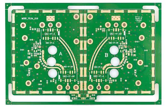
Multilayer Stack-Up Design for RF Transceiver PCB
Modern RF transceiver systems commonly use:
- Multilayer RF PCB architectures
- RF-digital hybrid stack-up structures
- Dedicated ground planes
- Shielding isolation layers
Proper stack-up design improves:
- Signal integrity
- RF isolation
- EMI suppression
- Routing efficiency
Optimized multilayer PCB structures reduce:
- Crosstalk interference
- RF signal leakage
- Power noise coupling
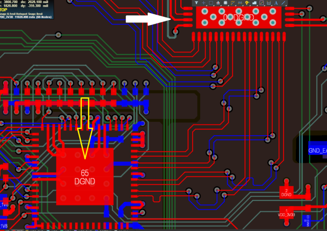
RF Layout Optimization
Proper RF PCB layout is one of the most important factors in wireless communication performance.
RF layout optimization techniques include:
- Short RF routing paths
- Smooth trace transitions
- Ground via stitching
- Antenna isolation optimization
- Controlled return current management
These methods improve:
- RF signal stability
- Antenna efficiency
- Communication reliability
EMI and EMC Optimization
RF communication systems are highly sensitive to electromagnetic interference.
EMI suppression strategies include:
- RF shielding structures
- Via fence isolation
- Layer separation optimization
- Differential routing techniques
- Ground plane management
Effective EMI control improves:
- Wireless communication quality
- RF transmission stability
- EMC compliance performance
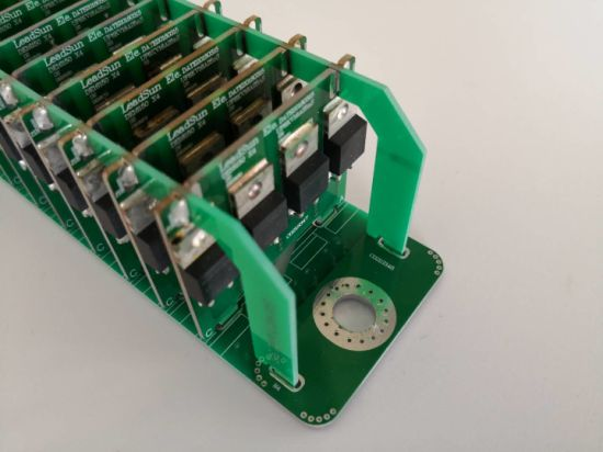
Thermal Management in RF Transceiver PCB
High-frequency RF systems generate concentrated heat from:
- RF amplifiers
- Power management ICs
- High-speed processors
- Wireless communication modules
Thermal management solutions include:
- Thermal via arrays
- Copper heat-spreading planes
- Heat sink integration
- Thermal balancing structures
Efficient thermal management improves:
- RF transmission stability
- System lifespan
- Communication reliability
Manufacturing Challenges of RF Transceiver PCB
RF Transceiver PCB fabrication requires advanced manufacturing precision.
Key manufacturing challenges include:
- Tight impedance tolerance control
- Precision RF trace processing
- Stable multilayer alignment
- Low-profile copper processing
- Consistent dielectric thickness control
High-frequency PCB manufacturing must minimize:
- Surface roughness variation
- Signal discontinuities
- RF transmission inconsistencies
At KKPCB, advanced manufacturing technologies ensure:
- Stable RF communication performance
- Reliable multilayer PCB quality
- Consistent microwave PCB production capability
Applications of RF Transceiver PCB
RF Transceiver PCB technology is widely used in:
- 5G communication systems
- Wireless networking devices
- Satellite communication equipment
- Automotive radar platforms
- IoT communication modules
- Aerospace RF electronics
- Smart wireless infrastructure
These applications require:
- Stable RF transmission
- Low-loss signal routing
- Reliable wireless communication performance
Future Trends in RF Transceiver PCB Technology
Future RF transceiver PCB development focuses on:
- 6G wireless communication systems
- AI-integrated RF modules
- mmWave wireless networking
- Ultra-high-density RF integration
- Compact smart communication platforms
Emerging technologies require:
- Faster wireless communication
- Better signal integrity
- Lower RF transmission loss
- More compact multilayer PCB architectures
Conclusion
RF Transceiver PCB technology is essential for modern:
- Wireless communication systems
- High-frequency networking platforms
- RF communication infrastructure
- Microwave electronic systems
Through optimized:
- Low-loss PCB materials
- RF multilayer stack-up design
- Signal integrity engineering
- EMI suppression techniques
- Advanced manufacturing precision
engineers can achieve:
- Stable wireless communication
- Better RF transmission quality
- Reduced signal loss
- Higher communication reliability
With extensive expertise in RF PCB engineering and microwave multilayer manufacturing, KKPCB delivers advanced PCB solutions for next-generation wireless communication technologies.
