1. Why RO4350B PCB Materials Are Widely Used
As modern electronic systems continue evolving toward:
- Higher operating frequencies
- Faster wireless communication
- Greater bandwidth demands
- Compact RF module integration
the need for advanced high-frequency PCB materials has rapidly increased.
Applications such as:
- 5G communication infrastructure
- Automotive radar systems
- RF transceiver modules
- Satellite communication equipment
- Aerospace microwave electronics
require PCB materials capable of maintaining:
- Low insertion loss
- Stable signal integrity
- Reliable impedance control
- Strong thermal stability
Traditional FR4 PCB materials often experience:
- Excessive dielectric loss
- Higher RF signal attenuation
- Reduced transmission quality at microwave frequencies
To solve these challenges, engineers increasingly adopt RO4350B PCB materials for:
- RF communication systems
- Microwave PCB applications
- High-speed wireless electronics
- Controlled impedance multilayer PCB design
At KKPCB, advanced RO4350B PCB solutions are optimized for:
- Low-loss RF transmission
- High-frequency signal integrity
- Reliable multilayer PCB performance
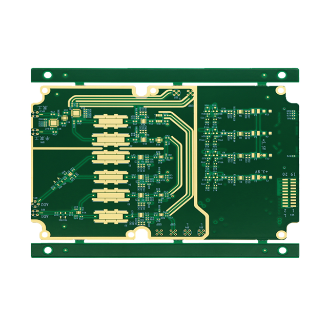
2. What Is RO4350B PCB?
RO4350B PCB is a high-frequency low-loss PCB material widely used in:
- RF electronics
- Microwave communication systems
- High-speed digital applications
RO4350B PCB materials provide:
- Low dielectric loss
- Stable dielectric constant
- Excellent thermal reliability
- Good manufacturability
Compared with standard FR4 PCB materials, RO4350B PCB offers:
- Better RF signal integrity
- Lower insertion loss
- Improved controlled impedance stability
- More reliable high-frequency transmission performance
This makes RO4350B PCB highly suitable for:
- RF antenna systems
- Automotive radar modules
- High-speed communication hardware
- Aerospace RF electronics
3. Key Characteristics of RO4350B PCB
3.1 Low Dielectric Loss Performance
One of the most important advantages of RO4350B PCB materials is low dielectric loss.
Low-loss PCB performance helps:
- Reduce RF signal attenuation
- Improve communication efficiency
- Maintain stable microwave transmission
This is especially important in:
- 5G RF systems
- Radar communication modules
- Microwave transceiver circuits
3.2 Stable Dielectric Constant
RO4350B PCB materials provide:
- Consistent dielectric properties
- Predictable RF transmission behavior
- Reliable impedance control capability
These characteristics improve:
- Signal integrity
- RF matching accuracy
- Microwave circuit stability
3.3 Excellent Controlled Impedance Performance
Controlled impedance is critical for:
- RF communication systems
- High-speed digital circuits
- Microwave PCB routing
RO4350B PCB materials support:
- Stable transmission line impedance
- Reduced signal reflection
- Consistent RF signal propagation
At KKPCB, advanced multilayer stack-up optimization ensures:
- Accurate impedance consistency
- Stable RF signal transmission
- Better high-speed PCB performance
3.4 Excellent Thermal Reliability
RO4350B PCB materials provide:
- Stable thermal performance
- Good dimensional stability
- Reliable thermal cycling resistance
These properties improve:
- Long-term operational stability
- RF system reliability
- High-frequency electrical consistency
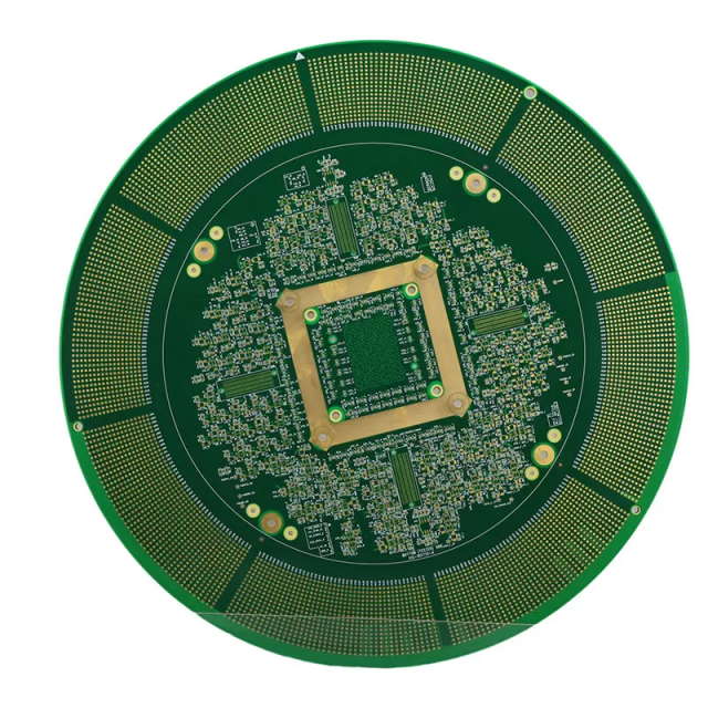
4. Applications of RO4350B PCB
RO4350B PCB technology is widely used in:
- 5G communication infrastructure
- Automotive radar systems
- RF power amplifiers
- Satellite communication modules
- Aerospace RF electronics
- Microwave antennas
- High-speed networking systems
These applications require:
- Low-loss RF transmission
- Stable signal integrity
- Reliable high-frequency performance
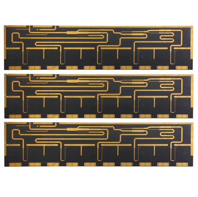
5. Multilayer Stack-Up Design for RO4350B PCB
Multilayer stack-up design directly affects:
- Signal integrity
- Controlled impedance consistency
- EMI suppression
- RF transmission efficiency
Important stack-up considerations include:
- Ground plane continuity
- Dielectric thickness control
- RF layer isolation
- Symmetrical multilayer structures
Optimized multilayer PCB structures improve:
- Crosstalk reduction
- RF shielding performance
- High-frequency transmission quality
6. RF Layout Optimization in RO4350B PCB
Proper RF layout significantly impacts:
- Signal integrity
- RF efficiency
- Microwave transmission quality
Best RF PCB design practices include:
- Short RF routing paths
- Smooth transmission line transitions
- Ground via stitching
- Controlled return current paths
- Isolation between RF and digital circuits
These techniques improve:
- RF communication stability
- Antenna performance
- High-frequency signal consistency
7. EMI and EMC Optimization
High-frequency RF systems generate substantial electromagnetic interference.
EMI suppression strategies include:
- Ground shielding structures
- RF via fences
- Differential routing optimization
- Layer isolation management
- Controlled return current paths
Effective EMI suppression improves:
- Signal quality
- Communication reliability
- EMC compliance performance
8. Thermal Management in RO4350B PCB
RF amplifiers and high-speed communication ICs generate concentrated heat.
Thermal management solutions include:
- Thermal via arrays
- Copper heat-spreading planes
- Heat sink integration
- Hybrid multilayer thermal structures
Efficient thermal design improves:
- RF stability
- Power efficiency
- Long-term reliability
9. Manufacturing Challenges of RO4350B PCB
RO4350B PCB fabrication requires advanced manufacturing precision.
Key manufacturing challenges include:
- Tight impedance tolerance control
- Precision RF trace geometry processing
- Stable dielectric thickness management
- Multilayer lamination consistency
- Low-profile copper processing
High-frequency PCB manufacturing must minimize:
- Signal discontinuities
- Surface roughness variation
- RF transmission inconsistencies
At KKPCB, advanced manufacturing technologies ensure:
- Stable electrical performance
- Reliable multilayer PCB quality
- Consistent high-frequency manufacturing capability
10. Advantages of RO4350B PCB Compared with Standard FR4
Compared with conventional FR4 PCB materials, RO4350B PCB offers:
- Lower dielectric loss
- Better signal integrity
- Improved RF transmission efficiency
- More stable impedance behavior
- Better thermal reliability
This makes RO4350B PCB ideal for:
- RF communication systems
- Microwave electronics
- Automotive radar applications
- High-speed wireless devices
11. Future Trends in RO4350B PCB Technology
Future RO4350B PCB development focuses on:
- mmWave communication systems
- Advanced automotive radar platforms
- AI-driven wireless communication infrastructure
- Compact RF module integration
- Higher multilayer routing density
Emerging technologies require:
- Faster wireless communication
- Lower insertion loss
- Better RF efficiency
- More advanced multilayer PCB structures
12. Conclusion
RO4350B PCB technology is an important solution for advanced:
- RF communication systems
- Microwave electronics
- High-speed wireless applications
Through optimized:
- Low-loss PCB materials
- Controlled impedance routing
- Signal integrity engineering
- Multilayer PCB stack-up design
- Advanced manufacturing precision
engineers can achieve:
- Stable RF transmission
- Better communication quality
- Reduced signal attenuation
- Higher system reliability
With extensive expertise in RF PCB engineering and microwave manufacturing, KKPCB delivers advanced low-loss PCB solutions for demanding wireless and aerospace applications.
