What Is an HDI PCB?
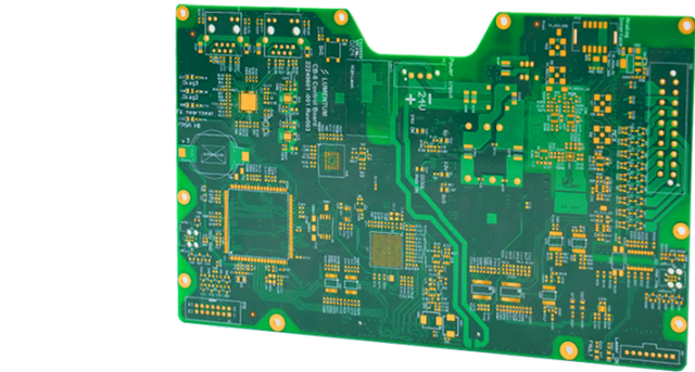
An HDI PCB (High Density Interconnect PCB) is a printed circuit board designed with higher wiring density per unit area compared to traditional PCBs. It typically incorporates microvias, blind and buried vias, fine trace widths, and advanced multilayer stack-ups to support compact and high-performance electronic designs.
HDI technology enables smaller product size, improved signal integrity, and enhanced electrical performance in modern electronic systems.
Key Features of HDI PCB
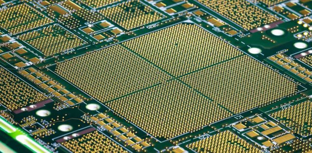
1. Microvia Technology
HDI PCBs use laser-drilled microvias, typically less than 150μm in diameter. Microvias:
-
Reduce via size
-
Increase routing density
-
Minimize parasitic inductance
-
Improve high-speed signal performance
Microvias are commonly used in sequential lamination structures.
2. Blind and Buried Vias
HDI structures often include:
-
Blind vias (connecting outer to inner layers)
-
Buried vias (connecting internal layers only)
These advanced via types optimize routing space and reduce surface congestion.
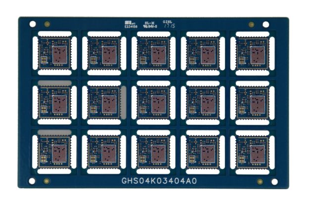
3. Fine Line and Fine Pitch Capability
HDI PCB supports:
-
Fine trace widths and spacing
-
High pin-count BGA packages
-
CSP and flip-chip components
This allows compact board layouts for high-performance devices.
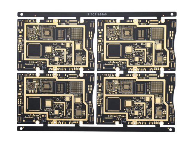
4. Sequential Lamination Process
HDI boards are typically manufactured using multiple lamination cycles to build layer-by-layer interconnections. This process enables:
-
Layer stacking flexibility
-
Microvia stacking
-
Improved interlayer reliability
Precise alignment control is critical during fabrication.
Advantages of HDI PCB
-
Smaller board size
-
Higher routing density
-
Better signal integrity
-
Reduced layer count in some designs
-
Improved electrical performance
-
Enhanced reliability for high-speed systems
HDI technology supports modern electronics that demand miniaturization and high performance.
Applications of HDI PCB
HDI PCBs are widely used in:
-
Smartphones and portable devices
-
Automotive electronics
-
5G communication equipment
-
Aerospace systems
-
Medical devices
-
UAV and robotics systems
-
Semiconductor test boards
As electronic systems become more compact and complex, HDI PCB adoption continues to grow.
HDI PCB vs Traditional Multilayer PCB
| Feature | Traditional PCB | HDI PCB |
|---|---|---|
| Via Type | Through-hole | Microvia + Blind/Buried |
| Routing Density | Moderate | High |
| Board Size | Larger | More Compact |
| Signal Performance | Standard | Improved |
| Manufacturing Complexity | Lower | Higher |
HDI PCBs require more advanced fabrication processes but deliver superior performance and integration.
Manufacturing Capabilities
Professional HDI PCB fabrication may include:
-
1+N+1 or 2+N+2 structures
-
Laser drilling
-
Sequential lamination
-
Via-in-pad plating
-
Controlled impedance verification
-
Fine line etching
-
X-ray inspection
Strict process control ensures reliable microvia integrity and layer alignment.
Conclusion
HDI PCB technology enables compact, high-performance electronic systems by integrating microvia structures, fine pitch routing, and advanced multilayer stack-ups. As product miniaturization and data speed requirements increase, HDI PCBs become essential in modern electronic design.
For automotive, communication, semiconductor testing, and industrial applications, HDI PCB provides a reliable and high-density interconnect solution.
