What Is HDI PCB?
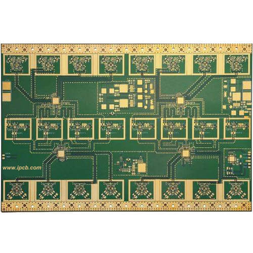
HDI PCB (High Density Interconnect PCB) is a printed circuit board designed with higher wiring density per unit area compared to traditional multilayer PCBs. It uses advanced manufacturing technologies such as microvias, blind vias, buried vias, and fine line traces to achieve compact size and improved electrical performance.
HDI PCB is widely used in modern electronic products that require miniaturization, high speed signal transmission, and complex routing structures.
Key Features of HDI PCB
1. Microvia Technology
HDI PCB typically uses laser drilled microvias with small diameters, allowing:
-
Higher routing density
-
Reduced signal path length
-
Improved electrical performance
-
Space-saving designs
Microvias can be stacked or staggered depending on design requirements.
2. Blind and Buried Vias
HDI PCB incorporates:
-
Blind vias (connecting outer to inner layers)
-
Buried vias (connecting inner layers only)
-
Via-in-pad structures
These features improve routing flexibility and allow high pin count components to be efficiently connected.
3. Fine Line and Fine Pitch Design
HDI PCB supports:
-
Fine line width and spacing
-
High pin count BGA packages
-
Small pitch components
-
High layer count stack-ups
This makes it ideal for advanced semiconductor packaging and compact device layouts.
4. Improved Signal Integrity
Compared with traditional PCB, HDI PCB offers:
-
Shorter signal paths
-
Reduced parasitic inductance
-
Better impedance control
-
Lower signal distortion
These advantages are critical for high speed digital and RF applications.
HDI PCB Manufacturing Capabilities
Advanced HDI PCB production may include:
-
4–20+ layer stack-ups
-
Sequential lamination processes
-
Laser drilling for microvias
-
Via filling and copper plating
-
Controlled impedance routing
-
High TG or low loss materials
-
Surface finishes such as ENIG, ENEPIG, immersion silver
Precise process control ensures reliability and dimensional accuracy.
Applications of HDI PCB
HDI PCB is widely used in:
-
Smartphones and tablets
-
5G communication devices
-
Automotive electronics and ADAS systems
-
Industrial control systems
-
Medical devices
-
Wearable electronics
-
High speed computing hardware
As electronic devices become smaller and more powerful, HDI PCB demand continues to increase.
Advantages of HDI PCB
-
Reduced board size and weight
-
Higher component density
-
Improved electrical performance
-
Better heat distribution
-
Enhanced design flexibility
-
Suitable for high pin count ICs
HDI PCB enables compact product design without sacrificing performance.
HDI PCB vs Traditional Multilayer PCB
| Feature | HDI PCB | Traditional PCB |
|---|---|---|
| Routing Density | Very High | Moderate |
| Via Structure | Microvia / Blind / Buried | Through Hole |
| Board Size | Smaller | Larger |
| Electrical Performance | Improved | Standard |
| Manufacturing Complexity | Higher | Lower |
HDI PCB is preferred for advanced and high performance electronic systems.
Conclusion
HDI PCB is a critical solution for modern electronics requiring compact size, high density routing, and reliable high speed performance. With microvia technology, advanced stack-up structures, and precise impedance control, HDI PCB supports next-generation communication, automotive, and semiconductor applications.
Choosing an experienced HDI PCB manufacturer ensures consistent quality, stable performance, and efficient production for complex electronic designs.
