What Is an RF Trace PCB?
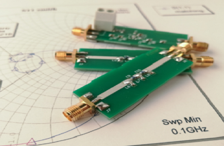
An RF Trace PCB is a printed circuit board designed to route high-frequency RF signals with minimal signal loss, reflection, and distortion. These PCBs are optimized for controlled impedance, low insertion loss, and high signal integrity, making them essential for applications such as 5G modules, mmWave systems, wireless communication, automotive radar, and RF transceivers.
Why RF Trace PCB Technology Matters
As wireless communication and high-frequency electronics evolve, traditional PCBs may fail to maintain signal quality. RF trace PCBs address critical challenges such as:
-
Signal attenuation at gigahertz frequencies
-
Impedance mismatch and reflection
-
Crosstalk and electromagnetic interference (EMI)
-
Dielectric losses and phase instability
-
Performance degradation over long traces
RF trace PCBs ensure reliable high-frequency signal transmission.
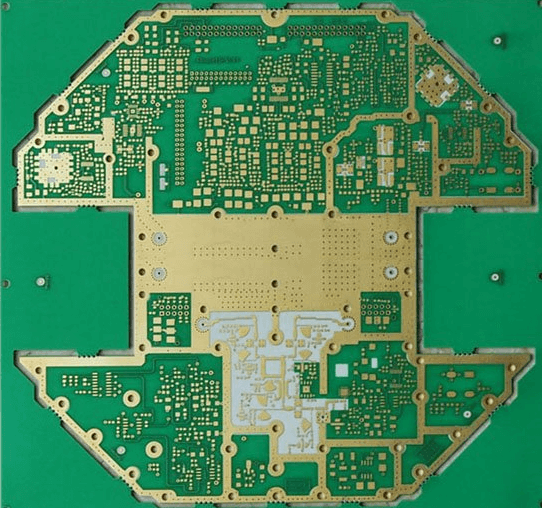
Key Features of RF Trace PCBs
High-quality RF trace PCBs typically include:
-
Controlled impedance traces for consistent signal propagation
-
Low-loss dielectric materials to minimize signal attenuation
-
Precision trace width and spacing for high-frequency stability
-
Optimized layer stackup and grounding
-
Microvias, blind/buried vias, and fine line routing for dense RF designs
These features guarantee high-frequency performance and signal integrity.
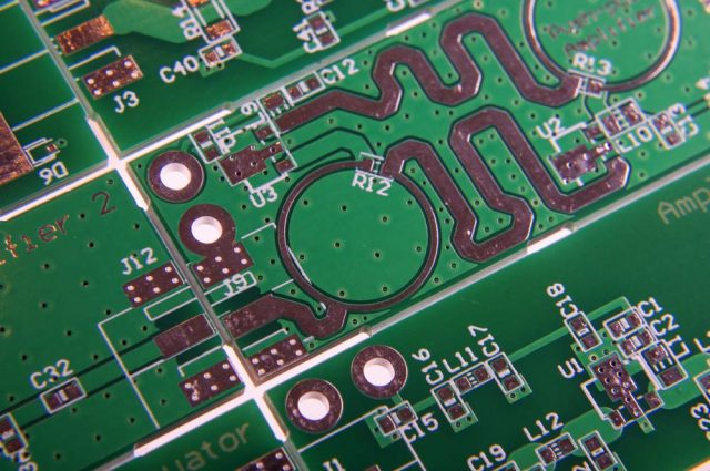
Design Considerations for RF Trace PCBs
Designing RF trace PCBs requires attention to:
-
Trace width and spacing calculation for controlled impedance
-
Short, direct signal paths to minimize loss
-
Crosstalk reduction through ground shielding and layer assignment
-
Microvia placement and fan-out for multilayer designs
-
Integration of RF connectors and filtering components
Careful design ensures minimal insertion loss and stable RF performance.
Materials for RF Trace PCBs
Material choice is critical for high-frequency signal performance:
-
Low-loss laminates such as Rogers RO4003C, RO4350B, Duroid 5880/6010, Taconic RF-35
-
High-TG FR-4 for hybrid high-speed circuits
-
Smooth copper foils to reduce conductor losses
-
Polyimide and hybrid materials for flexible RF layouts
Proper materials maintain signal integrity across wide frequency ranges.
Manufacturing Capabilities for RF Trace PCBs
RF trace PCB fabrication requires:
-
Precision etching and imaging for fine traces
-
Laser-drilled microvias for multilayer HDI designs
-
Tight layer-to-layer registration for impedance control
-
TDR and vector network analyzer (VNA) testing for RF validation
-
Automated optical inspection (AOI) and electrical testing
Professional manufacturing ensures consistent RF performance and reliability.
Assembly Considerations for RF Trace PCBs
Assembly of RF trace PCBs involves:
-
Accurate placement of RF components (antennas, filters, transceivers)
-
Controlled soldering profiles to preserve high-frequency traces
-
Shielding integration to reduce EMI
-
Functional testing for RF signal quality and insertion loss
-
ESD-safe handling for sensitive components
Proper assembly preserves RF signal integrity and device performance.
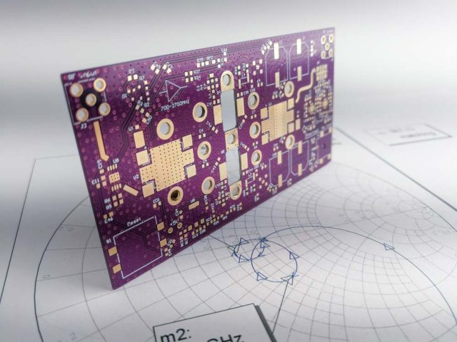
Applications of RF Trace PCBs
RF trace PCBs are widely used in:
-
5G and mmWave communication modules
-
Wireless transceivers and RF front-end modules
-
Automotive radar and ADAS electronics
-
Satellite and aerospace communication systems
-
High-speed RF test boards and semiconductor test systems
-
Industrial wireless sensors and IoT modules
They are essential wherever high-frequency, low-loss signal transmission is critical.
Why Choose a Professional RF Trace PCB Manufacturer
A professional RF PCB manufacturer provides:
-
Expertise in high-frequency PCB design and controlled impedance
-
Material selection for minimal dielectric and conductor loss
-
Prototype, small batch, and mass production support
-
Advanced RF testing (TDR, VNA) and inspection
-
One-stop PCB fabrication and assembly services
The right partner ensures high-frequency performance, signal integrity, and reliable wireless operation.
