An RF Trace PCB is a specialized printed circuit board designed for RF signal transmission and high-frequency applications, where signal loss, impedance stability, and EMI control are critical. As wireless technologies such as 5G, WiFi, GPS, IoT, and radar systems continue to grow, RF PCB performance requirements become stricter than ever.
Unlike ordinary digital traces, an RF trace behaves as a transmission line, meaning its physical geometry and stack-up structure directly affect the signal’s impedance, phase, attenuation, and radiation. That’s why RF Trace PCB design must combine controlled impedance routing, low-loss materials, and high-precision manufacturing to achieve stable high-frequency performance.
What Is an RF Trace PCB?
An RF Trace PCB refers to a PCB where the RF signal paths are carefully engineered to support high-frequency signals, typically from hundreds of MHz up to multiple GHz. These RF traces must maintain consistent impedance and minimize loss throughout the routing path.
Common RF trace routing structures include:
-
Microstrip PCB traces (outer-layer routing)
-
Stripline PCB traces (inner-layer routing)
-
Coplanar Waveguide (CPW) PCB traces
-
Grounded Coplanar Waveguide (GCPW) PCB traces
Each structure has different advantages in terms of EMI control, insertion loss, routing density, and manufacturability.
Why RF Trace PCB Design Is More Critical Than Standard PCB Routing
In high-speed digital routing, small discontinuities may still be acceptable. But in RF routing, even minor geometry changes can cause performance problems such as reflection, resonance, and unwanted radiation.
A professional RF Trace PCB design helps prevent:
-
Impedance mismatch and signal reflection
-
High insertion loss and attenuation
-
Crosstalk between RF and digital signals
-
EMI radiation and noise coupling
-
Frequency drift and unstable RF behavior
For RF communication products, stable RF trace performance directly impacts range, efficiency, sensitivity, and overall system reliability.
Key Requirements of RF Trace PCB Routing
1. Controlled Impedance for RF Traces
Controlled impedance is one of the most important targets in RF Trace PCB manufacturing. Typical RF impedance requirements include:
-
50Ω single-ended RF traces (most common)
-
75Ω RF traces (video and certain RF systems)
-
Differential impedance for specific RF and high-speed signal paths
Controlled impedance depends on:
-
Trace width and spacing
-
Dielectric thickness
-
Copper thickness
-
Material dielectric constant (Dk)
-
Stack-up structure and reference planes
Accurate impedance control ensures stable transmission, low reflection, and consistent RF performance.
2. Low Loss Performance for High-Frequency Signals
At high frequencies, signal loss becomes a major challenge. RF Trace PCB loss comes mainly from:
-
Dielectric loss (material dissipation factor Df)
-
Conductor loss (skin effect and copper roughness)
-
Radiation loss (poor shielding or routing)
To improve low-loss performance, RF Trace PCB designs often require low-loss PCB materials, optimized stack-ups, and smooth routing transitions.
3. Stable Grounding and Return Path Control
RF signals require clean and continuous return paths. A good RF Trace PCB layout typically includes:
-
Solid ground planes under RF traces
-
Short return paths and minimized loop area
-
Via stitching and ground fencing around RF routes
-
Stable reference plane transitions between layers
Strong grounding improves impedance stability, reduces EMI, and supports better RF shielding.
4. RF Trace Geometry and Routing Consistency
In RF Trace PCB routing, geometry consistency is essential. Good RF routing practices include:
-
Keeping trace width constant
-
Avoiding sharp 90° corners (use arcs or 45° bends)
-
Minimizing routing length when possible
-
Avoiding sudden neck-downs or widening
-
Using smooth transitions for pads and connectors
Even small geometry changes can create impedance discontinuities and reflections.
RF Trace PCB Stack-Up Options
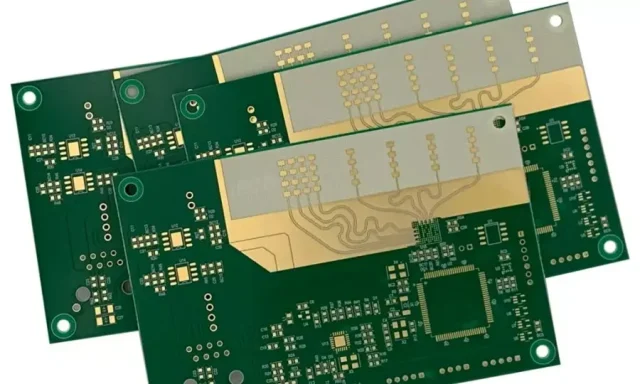
RF Trace PCB performance depends heavily on stack-up design. Common stack-up approaches include:
Microstrip RF Trace PCB
Microstrip traces run on the outer layer with a ground reference plane below. Advantages:
-
Easy to probe and tune
-
Simple manufacturing
-
Suitable for antennas and RF front-end circuits
Stripline RF Trace PCB
Stripline traces run on inner layers between two reference planes. Advantages:
-
Better EMI shielding
-
Lower radiation
-
More stable impedance environment
CPW / GCPW RF Trace PCB
Coplanar waveguide structures place ground copper near the trace on the same layer. Advantages:
-
Stronger impedance control
-
Better EMI containment
-
Common in 5G and compact RF modules
RF Trace PCB Material Selection
Choosing the right PCB material is essential for RF trace performance. Depending on frequency and loss targets, RF Trace PCBs may use:
-
FR-4 (for lower-frequency RF or cost-sensitive designs)
-
Rogers PCB materials (RO4003C, RO3003, etc.)
-
Duroid PCB materials (PTFE-based for microwave applications)
-
Megtron PCB materials (low loss for mixed high-speed + RF designs)
For high-frequency signal PCB requirements, low-loss materials provide better insertion loss control and more stable performance.
RF Trace PCB Manufacturing Considerations
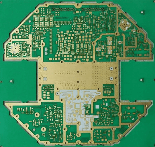
RF Trace PCB manufacturing requires tighter control than standard PCB production. Key process points include:
-
Tight etching tolerance for trace width and spacing
-
Stable dielectric thickness control for impedance accuracy
-
Copper roughness control to reduce conductor loss
-
Layer alignment and registration for multilayer RF PCBs
-
High-reliability plating for vias and ground stitching
-
Controlled impedance testing and verification
Manufacturing precision directly impacts RF signal quality, especially at GHz-level frequencies.
Typical Applications of RF Trace PCB
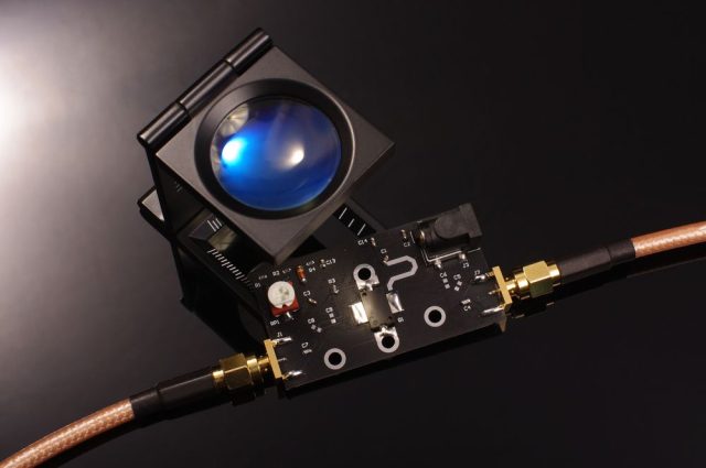
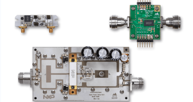
RF Trace PCBs are widely used in advanced electronics such as:
-
5G RF modules and wireless communication systems
-
WiFi / Bluetooth devices and routers
-
GPS receivers and positioning modules
-
RF front-end modules (FEM)
-
Antenna feed networks and matching circuits
-
Automotive radar and ADAS RF systems
-
IoT wireless sensor modules
-
Microwave test boards and RF measurement equipment
In all these applications, RF Trace PCB routing quality directly affects system performance.
KKPCB RF Trace PCB Manufacturing Capabilities
KKPCB provides professional RF Trace PCB manufacturing services for high-frequency applications, including:
-
Controlled impedance RF Trace PCB fabrication
-
Low-loss material support (Rogers, Megtron, hybrid stack-ups)
-
Fine line routing for compact RF modules
-
Multilayer RF Trace PCB production
-
High reliability inspection and electrical testing
-
Engineering support for stack-up planning and DFM review
From prototype to mass production, KKPCB helps customers achieve stable RF performance with consistent manufacturing quality.
Conclusion
An RF Trace PCB is essential for high-frequency and RF communication products that require controlled impedance, low loss, and stable signal integrity. With proper routing rules, optimized stack-up design, and precision manufacturing, RF Trace PCBs can deliver reliable performance for 5G, WiFi, GPS, IoT, radar, and advanced wireless systems.
KKPCB supports high-quality RF Trace PCB fabrication with engineering expertise, controlled impedance capability, and high-reliability production control to meet demanding RF design requirements.
