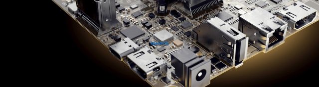
What Is a Fine Line PCB?

A Fine Line PCB is a high-precision printed circuit board manufactured with ultra-thin trace width and tight trace spacing, enabling high-density routing for advanced electronic products. Compared with standard PCB technology, Fine Line PCB fabrication focuses on achieving smaller line/space (L/S), higher wiring density, and improved signal performance in compact designs.
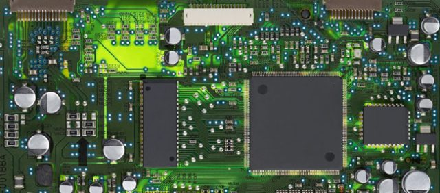
Fine Line PCBs are widely used in HDI PCB designs, fine pitch component layouts, high-speed digital systems, and high-frequency electronics, where routing space is limited and signal integrity requirements are strict.
Why Fine Line PCB Technology Is Important
As modern electronics become smaller and faster, designers must route more signals into less space while keeping stable performance. Fine Line PCB technology supports:
-
High-density interconnection (HDI) for compact layouts
-
Fine pitch PCB assembly for small-pitch ICs and BGAs
-
Better routing capability for high-speed digital signals
-
Improved layout flexibility for complex multilayer boards
-
Reduced risk of routing congestion in dense designs
A Fine Line PCB is often the key solution for products that require miniaturization without sacrificing performance.
Key Advantages of Fine Line PCB
1. Higher Routing Density
Fine Line PCBs allow more signal traces to be routed between component pads, especially in designs using:
-
Fine pitch ICs
-
High pin-count BGAs
-
Dense connectors and interfaces
This makes Fine Line PCB routing ideal for compact, high-density PCB layouts.
2. Support for HDI PCB and Microvia Technology
Fine Line PCB fabrication is commonly combined with HDI PCB structures such as:
-
Microvia PCB designs
-
Blind via and buried via PCB
-
Via-in-pad technology
This combination enables higher interconnect density and shorter signal paths for high-performance electronics.
3. Better Signal Integrity for High-Speed Designs
A Fine Line PCB can improve high-speed performance by enabling:
-
Shorter routing paths
-
Cleaner trace geometry
-
Better controlled impedance routing
-
Reduced parasitic effects in dense layouts
With optimized stack-up and controlled impedance, Fine Line PCBs help maintain strong signal integrity in high-speed digital applications.
4. Improved Layout Flexibility
Fine Line PCB technology gives engineers more freedom to:
-
Optimize component placement
-
Reduce layer count in some designs
-
Improve routing efficiency
-
Achieve compact product dimensions
This helps shorten development cycles and reduce redesign risks.
5. Compatibility with Multilayer PCB Structures
Fine Line PCBs are often built as multilayer PCBs, including 6-layer, 8-layer, 10-layer, and higher layer counts. Multilayer Fine Line PCB design supports:
-
Better grounding and shielding
-
Improved EMI control
-
Stable reference planes for high-speed signals
-
Advanced power distribution networks
Typical Applications of Fine Line PCB
Fine Line PCBs are widely used in electronics that require high-density routing and high precision manufacturing, including:
-
HDI PCB for smartphones and wearable devices
-
High-speed networking equipment (routers, switches, servers)
-
5G communication modules and RF systems
-
Automotive electronics and ADAS systems
-
Industrial automation control boards
-
Medical electronics with compact layouts
-
IC test PCB and ATE test boards
-
High-speed logic PCBs with dense routing
Fine Line PCB Manufacturing Challenges
Producing a Fine Line PCB requires strict process control and stable manufacturing capability. Common challenges include:
-
Tight tolerance for trace width and spacing
-
Higher risk of open/short defects in fine features
-
Increased difficulty in etching and plating control
-
Higher requirements for AOI inspection and quality control
-
Strong demand for stable lamination and registration accuracy
To ensure consistent quality, Fine Line PCB manufacturing must be supported by advanced equipment and experienced engineering control.
KKPCB Fine Line PCB Manufacturing Capabilities
KKPCB provides professional Fine Line PCB manufacturing with strong engineering support for high-density and high-precision projects. Our capabilities include:
-
High precision Fine Line PCB fabrication
-
Multilayer Fine Line PCB production
-
HDI PCB and microvia PCB processing options
-
Controlled impedance PCB manufacturing for high-speed signals
-
High reliability PCB quality control and inspection
-
Prototype to mass production support
-
DFM review to improve yield and manufacturability
We help customers achieve stable performance and reliable production quality for Fine Line PCB designs.
Conclusion
A Fine Line PCB is a key technology for modern electronics requiring high-density routing, compact design, and high precision manufacturing. With ultra-thin traces, tight spacing, and compatibility with HDI and multilayer structures, Fine Line PCBs support advanced applications such as 5G, networking, automotive electronics, and high-speed digital systems.
KKPCB delivers high-quality Fine Line PCB solutions with controlled manufacturing processes, ensuring excellent performance, reliability, and production consistency for demanding products.
