What Is a Power Integrity PCB?
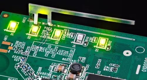
A Power Integrity PCB is a printed circuit board engineered to deliver stable voltage, low-noise power, and reliable current distribution to high-speed ICs such as CPUs, GPUs, FPGAs, ASICs, and high-density memory devices. In modern electronics, core voltages are getting lower while current demand is increasing, which makes power integrity (PI) a critical factor in overall system performance.
A well-designed Power Integrity PCB reduces PDN impedance, controls voltage ripple, minimizes transient voltage droop, and prevents power noise from coupling into sensitive signal paths. Power integrity directly impacts signal integrity, EMI performance, thermal stability, and product reliability, especially in high-speed and high-current applications.
Why Power Integrity Matters in High-Speed Electronics
In high-speed systems, the load current can change extremely fast. If the PCB power delivery network cannot respond quickly, the power rail will experience instability. Poor power integrity can cause:
-
Voltage droop during load transients
-
Voltage ripple and switching noise
-
Ground bounce and reference instability
-
Timing margin loss and increased jitter
-
Random resets and system crashes
-
Higher EMI emissions and compliance risks
-
Reduced reliability for long-term operation
That’s why Power Integrity PCB design is essential for high-speed products where stable power is required under dynamic load conditions.
Key Design Elements of a Power Integrity PCB
1. Low-Impedance PDN (Power Delivery Network)
A high-quality Power Integrity PCB is built around a low-impedance PDN. The goal is to keep PDN impedance low across a wide frequency range so the power rail remains stable during high-speed switching.
A low-impedance PDN helps reduce:
-
Transient voltage droop
-
Power rail noise
-
High-frequency ripple
-
Power-related signal distortion
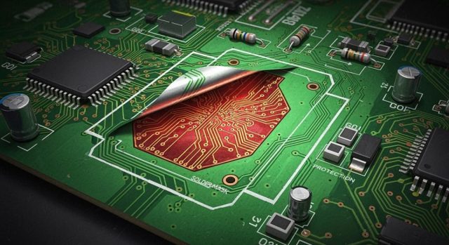
2. Optimized Multilayer Stack-Up
A professional multilayer PCB stack-up is one of the most effective ways to improve power integrity. A Power Integrity PCB stack-up typically includes:
-
Solid power planes and ground planes
-
Tight plane spacing to increase plane capacitance
-
Dedicated reference planes for high-speed signals
-
Reduced loop inductance for stable current return paths
An optimized stack-up improves power stability, noise suppression, and EMI control.
3. Decoupling Capacitor Strategy
A Power Integrity PCB requires correct decoupling at different frequency ranges. A complete decoupling strategy often includes:
-
Bulk capacitors for low-frequency stability
-
Mid-frequency capacitors for dynamic load changes
-
High-frequency capacitors placed close to IC power pins
Proper decoupling helps maintain stable voltage and reduces PDN resonance issues.
Key best practices for decoupling on a Power Integrity PCB:
-
Place capacitors close to the power pins
-
Use short, wide connections to reduce inductance
-
Use multiple capacitor values to cover a wide frequency range
-
Ensure a solid return path to the ground plane
4. Power Plane and Ground Plane Design
A Power Integrity PCB relies heavily on plane design. A stable power distribution system requires:
-
Continuous power planes with minimal splits
-
Strong ground reference for stable return current paths
-
Proper separation of noisy power rails and sensitive rails
-
Reduced plane discontinuities that cause impedance jumps
A stable power plane PCB design improves voltage stability and reduces EMI risks.
5. High Current Routing and Copper Thickness
Many Power Integrity PCBs must support high current rails such as 5V, 12V, or low-voltage high-current cores. To handle high current safely, designers often use:
-
Wider traces or copper pours
-
Thicker copper (e.g., 2oz, 3oz, or higher)
-
Multiple parallel traces for current sharing
-
Proper thermal relief and heat spreading
A Power Integrity PCB must ensure low resistance, low temperature rise, and reliable current delivery.
6. Via Design for Power Delivery
Vias play a major role in power integrity. Poor via design increases inductance and reduces PDN performance. A Power Integrity PCB often uses:
-
Multiple vias in parallel for power and ground connections
-
Via arrays for high-current power transfer between layers
-
Short via paths to reduce inductive effects
-
Strong stitching vias to stabilize ground reference
Optimized via design improves PDN performance and power rail stability.
7. Minimizing EMI and Noise Coupling
Power integrity is closely related to EMI. A noisy power rail can radiate EMI and disturb sensitive circuits. A Power Integrity PCB improves EMI performance by:
-
Using solid ground planes for shielding
-
Reducing current loop areas
-
Placing decoupling capacitors correctly
-
Separating switching power sections from sensitive signals
-
Using proper return path design
Better power integrity reduces EMI emissions and noise coupling, improving compliance success rate.
Typical Applications of Power Integrity PCBs
Power Integrity PCBs are widely used in systems that require stable power delivery and high reliability, such as:
-
Servers and data center hardware
-
High-speed networking switches and routers
-
5G base stations and communication modules
-
Automotive electronics (ECU, ADAS, radar systems)
-
Industrial automation and control systems
-
Aerospace and defense electronics
-
IC test PCB and ATE test boards
-
High-current power control modules
KKPCB Power Integrity PCB Manufacturing Capabilities
KKPCB provides professional Power Integrity PCB manufacturing with engineering support to help customers achieve stable power performance. Our capabilities include:
-
Multilayer PCB fabrication for complex PDN designs
-
High current PCB manufacturing with thick copper options
-
Optimized stack-up support for power and ground plane performance
-
Controlled impedance PCB capability for SI + PI combined designs
-
HDI PCB and fine line PCB for dense power routing
-
Via arrays and stitching via processing for strong PDN connections
-
High reliability testing for stable production quality
We support prototype to mass production, ensuring every Power Integrity PCB meets strict requirements for power stability, reliability, and long-term performance.
Conclusion
A Power Integrity PCB is essential for high-speed and high-current electronics, ensuring stable voltage, low noise, and reliable power delivery. By optimizing PDN impedance, stack-up design, decoupling capacitor placement, power plane layout, and via strategy, a Power Integrity PCB improves system stability, EMI performance, and product reliability.
KKPCB delivers high-quality Power Integrity PCB solutions for demanding applications such as 5G, data centers, automotive electronics, industrial control, and IC test systems.
