What Is a High Frequency Signal PCB?
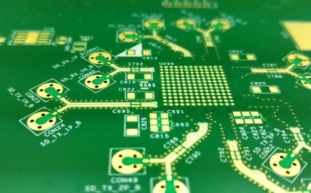
A High Frequency Signal PCB is a printed circuit board specifically engineered to handle high-speed and high-frequency signals with minimal signal loss and optimal signal integrity. These PCBs are crucial in RF communication, 5G modules, high-speed computing, IoT devices, and automotive radar systems.
High frequency signals require careful trace design, impedance control, and material selection to avoid signal degradation, reflections, and crosstalk.
Why High Frequency Signal PCBs Are Essential
High frequency signals present unique challenges:
-
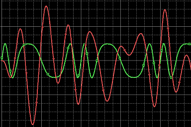
Signal integrity issues due to reflections and noise
-
Crosstalk and EMI between adjacent traces
-
Insertion loss in long traces or high-speed routes
-
Thermal management for power handling and reliability
Properly designed High Frequency Signal PCBs ensure stable performance, minimal interference, and high-speed operation, essential for modern electronic devices.
Key Design Considerations for High Frequency Signal PCBs
1. Controlled Impedance
High frequency traces require precise impedance matching using accurate trace widths, spacing, and dielectric constants. Controlled impedance ensures low reflection, minimal signal distortion, and stable performance.
2. Low-Loss Materials
Selecting low-loss laminates like Rogers, Taconic, or PTFE reduces dielectric attenuation and insertion loss, preserving high-frequency signal strength.
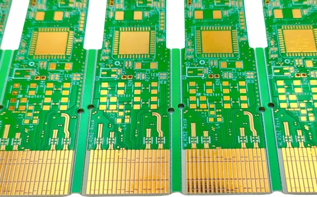
3. Multilayer Stack-Up Optimization
High frequency PCBs often use multilayer designs with dedicated ground and power planes, providing stable return paths, reduced EMI, and improved signal integrity.
4. Trace Routing and Layout
Careful trace routing, microstrip or stripline configurations, and differential pair routing reduce crosstalk and maintain signal quality.
5. Thermal and Power Management
High-speed traces may carry substantial currents. Proper copper thickness, thermal vias, and heat dissipation techniques maintain reliability and prevent overheating.
6. High-Precision Manufacturing
Advanced etching, inspection, and process control ensure repeatable quality, even in fine-pitch, high-density, or high-layer-count PCBs.
Applications of High Frequency Signal PCBs
-
5G and high-speed wireless communication modules
-
RF front-end circuits for smartphones and IoT devices
-
Automotive radar and advanced driver-assistance systems (ADAS)
-
High-speed computing and server motherboards
-
IoT devices and compact wearable electronics
-
Aerospace and defense communication systems
KKPCB High Frequency Signal PCB Capabilities
KKPCB provides professional high frequency signal PCB services, including:
-
Controlled impedance and differential pair routing
-
Low-loss material selection for RF and high-speed applications
-
Multilayer and HDI PCB fabrication
-
Crosstalk mitigation and EMI reduction
-
Thermal management and power handling optimization
-
Prototyping and mass production services
Our engineering team ensures every High Frequency Signal PCB meets strict electrical, thermal, and mechanical specifications, delivering high-speed, high-frequency, and reliable performance.
Conclusion
A High Frequency Signal PCB is vital for modern high-speed electronics, RF, 5G, IoT, and automotive systems. By combining controlled impedance, low-loss materials, multilayer optimization, and precise trace routing, KKPCB provides professional high-frequency PCB solutions that ensure signal integrity, reliability, and optimal electronic performance.
