What Is a Signal Integrity PCB?
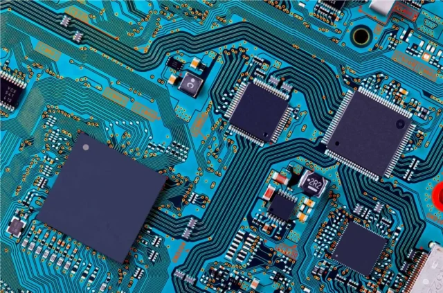
A Signal Integrity PCB is engineered to maintain clean, reliable, and distortion-free signal transmission in high-speed and high-frequency electronic systems. Signal degradation, crosstalk, and reflections can compromise system performance, especially in high-speed digital, RF, 5G, IoT, and high-performance computing applications.
Signal integrity PCB design ensures consistent impedance, controlled trace geometry, and proper layer stack-ups, minimizing interference and maintaining reliable data transmission.
Why Signal Integrity Is Critical
Modern electronic systems operate at multi-gigabit speeds, and even small impedance mismatches or layout errors can result in:
-
Signal reflections and ringing
-
Timing errors in high-speed interfaces
-
Crosstalk between adjacent traces
-
Power integrity issues impacting performance
Maintaining signal integrity is essential for reliable operation, system stability, and regulatory compliance.
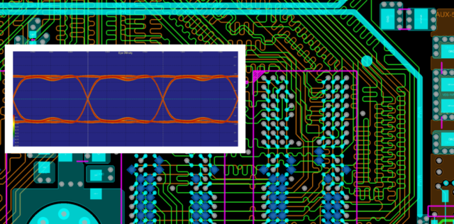
Key Design Considerations for Signal Integrity PCBs
-
Controlled Impedance:
-
Ensures consistent signal velocity and reduces reflections
-
Critical for differential pairs and high-speed traces
-
-
Differential Pair Routing:
-
Minimizes noise and electromagnetic interference (EMI)
-
Maintains high-speed data transmission accuracy
-
-
Layer Stack-Up Optimization:
-
Dedicated ground and power planes reduce loop area
-
Improves return path and minimizes EMI
-
-
Trace Spacing and Width:
-
Optimized for high-speed signals and low crosstalk
-
Fine-pitch routing for high-density applications
-
-
Material Selection:
-
Low-loss laminates and high-Tg substrates maintain signal integrity
-
Suitable for RF, high-frequency, and high-speed digital circuits
-
Applications of Signal Integrity PCBs
-
High-speed computing and data centers
-
Telecommunication and 5G modules
-
IoT devices with high-speed data interfaces
-
Automotive advanced driver-assistance systems (ADAS)
-
RF and mixed-signal electronics
KKPCB Signal Integrity PCB Capabilities
KKPCB provides full-service signal integrity PCB solutions, including:
-
Multilayer PCB fabrication with controlled impedance
-
Differential pair routing and high-speed trace design
-
Low-loss material selection for high-frequency applications
-
Fine-pitch, high-density HDI PCB manufacturing
-
Comprehensive electrical testing and quality assurance
Our engineers ensure optimal signal integrity, minimal EMI, and reliable performance, from prototype to volume production.
Conclusion
A Signal Integrity PCB is essential for modern high-speed electronics where noise, crosstalk, and signal degradation cannot be tolerated. Through precise design, controlled impedance, and advanced manufacturing, KKPCB delivers high-performance, reliable PCBs that meet the demands of industrial, automotive, RF, and high-frequency applications.
