What Is a Signal Integrity PCB?
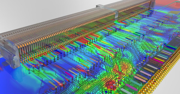
A Signal Integrity (SI) PCB is a printed circuit board designed to maintain clean, stable high-speed signal transmission across digital, analog, or mixed-signal circuits. SI PCBs are essential for applications where data integrity, minimal signal distortion, and timing accuracy are critical, such as 5G communications, high-speed computing, automotive electronics, and semiconductor testing.
Why Signal Integrity PCB Technology Matters
With increasing data rates and shrinking signal rise times, traditional PCB designs often suffer from:
-
Signal reflection and impedance mismatch
-
Crosstalk between traces
-
Insertion loss and dielectric loss
-
Timing skew and signal distortion
-
EMI/EMC interference
Signal integrity PCBs are engineered to overcome these issues, ensuring reliable and accurate signal transmission.
Key Features of Signal Integrity PCBs
A high-quality SI PCB typically includes:
-
Controlled impedance traces for matched signal lines
-
Low loss dielectric materials for high-frequency performance
-
Optimized trace width, spacing, and routing
-
Ground and power plane optimization
-
Shielding and isolation for sensitive signals
These features help maintain signal fidelity even in high-speed, high-density applications.
Design Considerations for Signal Integrity PCBs
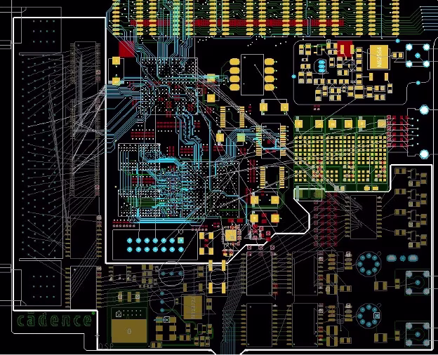
Effective SI PCB design requires attention to:
-
Trace length matching for high-speed buses
-
Differential pair routing for DDR, USB, PCIe, and Ethernet
-
Crosstalk reduction through spacing and shielding
-
Layer stackup optimization for impedance and return paths
-
Minimization of vias and signal discontinuities
Early design analysis ensures reliable high-speed performance in production.
Materials for Signal Integrity PCBs
Material selection is crucial for SI performance:
-
Low loss laminates such as Rogers, RO4003C, RO4350B, Duroid, Taconic RF-35
-
High-TG FR-4 for thermal stability in mixed-speed applications
-
Hybrid materials for RF, analog, and digital integration
-
Copper foil with smooth surfaces for low insertion loss
Right material choice ensures consistent impedance and low signal attenuation.
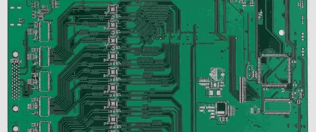
Manufacturing Capabilities for Signal Integrity PCBs
Producing SI PCBs requires advanced manufacturing technologies:
-
Tight control of trace width and spacing
-
Impedance verification with TDR testing
-
High-precision multilayer lamination
-
Laser-drilled microvias and HDI capability
-
Automated optical inspection (AOI) and electrical testing
Strict process control guarantees high-speed signal performance and reliability.
Assembly Considerations for Signal Integrity PCBs
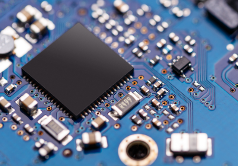
Assembly of SI PCBs involves:
-
Fine-pitch and high-density component placement
-
Controlled reflow and soldering for minimal thermal stress
-
Differential pair routing preservation during assembly
-
Shielded connector and component integration
-
Functional high-speed signal testing
Professional assembly preserves signal integrity and performance.
Applications of Signal Integrity PCBs
SI PCBs are widely used in:
-
High-speed computing and server boards
-
5G/6G communication and mmWave modules
-
High-speed data acquisition and test equipment
-
Automotive ADAS and infotainment electronics
-
Semiconductor test boards and load boards
-
Industrial automation and robotics
They are critical wherever high-speed, accurate signal transmission is required.
Why Choose a Professional Signal Integrity PCB Manufacturer
A professional SI PCB manufacturer provides:
-
Expertise in high-speed PCB design and controlled impedance
-
Material and stackup selection for minimal signal loss
-
Consistent quality for prototypes and mass production
-
Advanced inspection, testing, and validation
-
End-to-end PCB fabrication and assembly support
The right partner ensures reliable signal transmission, reduced noise, and long-term system stability.
