RO4003C PCB is a high-performance printed circuit board fabricated using Rogers RO4003C laminates, a leading low-loss material designed for high-frequency, RF, and microwave applications. Compared with conventional FR-4, RO4003C PCB provides lower dielectric loss, stable dielectric constant (Dk), and excellent controlled impedance, making it ideal for applications that require high signal integrity and minimal insertion loss.
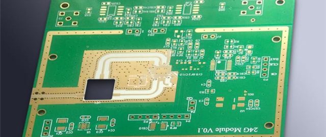
RO4003C PCB is widely used in RF modules, microwave circuits, 5G communication systems, WiFi routers, GPS devices, radar, and high-speed digital applications. Its superior electrical and thermal properties ensure stable performance at GHz frequencies and reliable operation in demanding environments.
Key Features of RO4003C PCB
1. Low Dielectric Loss
RO4003C PCB features a low dissipation factor (Df), which reduces insertion loss and signal attenuation. This is critical for maintaining signal strength in high-frequency applications and ensuring consistent RF performance.
2. Stable Dielectric Constant (Dk)
RO4003C laminates maintain a stable dielectric constant across a wide frequency range and temperature spectrum, providing predictable controlled impedance and reducing signal reflection.
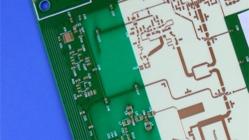
3. Controlled Impedance
Precise impedance control is essential in high-frequency designs. RO4003C PCB allows engineers to achieve exact 50Ω, 75Ω, or differential impedance targets, improving signal integrity and minimizing crosstalk.
4. Thermal and Mechanical Stability
With low coefficient of thermal expansion (CTE), RO4003C PCB ensures reliable multilayer lamination, stable vias, and minimal dimensional changes, even in high-temperature or high-density designs.
5. Excellent High-Frequency Performance
RO4003C PCB supports high-frequency signals with minimal loss, making it suitable for:
-
5G communication modules
-
WiFi and Bluetooth devices
-
GPS and navigation systems
-
Radar and automotive ADAS modules
-
Microwave circuits and antenna networks
-
High-speed differential signal networks (PCIe, Ethernet, SerDes)
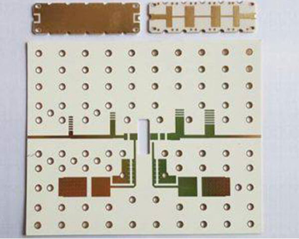
RO4003C PCB Manufacturing Considerations
Manufacturing RO4003C PCB requires precise process control:
-
Tight trace width and spacing to maintain impedance
-
Consistent dielectric thickness for stable Dk
-
Optimized copper roughness to minimize conductor loss
-
Accurate multilayer lamination for stack-up reliability
-
Controlled via and pad design to reduce reflection and insertion loss
-
Electrical testing to verify impedance, insertion loss, and return loss
KKPCB offers professional RO4003C PCB fabrication, from prototype to mass production, with engineering support for stack-up design, DFM, and controlled impedance verification.
Applications of RO4003C PCB
RO4003C PCB is ideal for industries requiring low-loss, high-frequency, and controlled impedance performance:
-
5G communication and base stations
-
WiFi and Bluetooth modules
-
GPS and navigation systems
-
Radar and automotive sensors
-
Satellite and microwave communication
-
IoT wireless devices
-
RF front-end modules
-
High-speed networking boards
-
Antenna feed networks and matching circuits
Conclusion
RO4003C PCB is a reliable solution for high-frequency, RF, microwave, and high-speed applications, providing low loss, stable Dk, and controlled impedance for superior signal integrity. With RO4003C PCB, engineers can achieve consistent performance in 5G, WiFi, radar, GPS, and microwave systems.
KKPCB provides RO4003C PCB manufacturing with advanced engineering support, multilayer stack-up capabilities, and strict quality control to ensure high-frequency performance from prototype to mass production.
