What Is an RF Trace PCB?
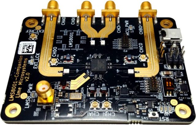
An RF Trace PCB is a printed circuit board designed specifically to carry high-frequency radio signals with minimal signal loss, low crosstalk, and controlled impedance. These PCBs are critical in RF communication, 5G modules, Wi-Fi, IoT devices, and high-speed signal processing.
RF Trace PCBs ensure that signal integrity, frequency response, and power handling are maintained in applications where even small signal degradation can impact performance.
Why RF Trace PCBs Are Important
High-frequency signals are prone to loss, reflection, and interference. Proper RF trace design ensures:
-
Consistent impedance matching
-
Reduced signal loss and attenuation
-
Minimal crosstalk and EMI
-
Reliable high-speed and high-frequency operation
These benefits are crucial for 5G, IoT, radar modules, RF front-end circuits, and high-speed wireless communication systems.
Key Design Considerations for RF Trace PCBs
1. Controlled Impedance
Precise trace width, spacing, and dielectric selection maintain characteristic impedance, ensuring signal integrity across high-frequency paths.
2. Low-Loss Materials
High-frequency signals require low-loss laminates (e.g., Rogers, Taconic, or PTFE) to minimize insertion loss and dielectric attenuation.
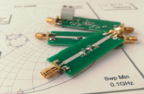
3. Trace Geometry and Routing
Proper microstrip or stripline routing, along with careful trace length matching, ensures signal stability and reduces reflections.
4. Crosstalk and Noise Mitigation
Maintaining adequate separation between RF traces and using ground planes strategically reduces crosstalk and EMI.
5. Thermal and Power Considerations
High-frequency traces often carry power for RF circuits. Adequate copper thickness, thermal vias, and heat dissipation techniques ensure performance and longevity.
6. Multilayer Stack-Up Optimization
RF PCBs often use multilayer structures to separate signal, ground, and power planes, providing stable return paths and controlled electromagnetic behavior.
Applications of RF Trace PCBs
-
5G wireless communication modules
-
IoT and wearable RF devices
-
Wi-Fi, Bluetooth, and other high-frequency wireless systems
-
RF front-end modules for smartphones and base stations
-
Automotive radar and sensor systems
-
High-speed test and measurement equipment
KKPCB RF Trace PCB Capabilities
KKPCB provides professional RF Trace PCB design and manufacturing services, including:
-
Controlled impedance and differential pair routing
-
Low-loss material selection (Rogers, Taconic, PTFE)
-
Multilayer PCB fabrication with optimized stack-ups
-
Crosstalk mitigation and EMI reduction
-
Thermal and power management solutions
-
Prototyping to high-volume production
Our engineering team ensures that every RF Trace PCB meets stringent electrical, thermal, and mechanical requirements, delivering reliable high-frequency performance.
Conclusion
A well-designed RF Trace PCB is critical for high-frequency, high-speed, and RF electronics. With controlled impedance, low-loss materials, precise routing, and multilayer stack-ups, KKPCB provides professional RF PCB solutions for 5G, IoT, automotive radar, and wireless communication systems.
