Why Low Dissipation Factor PCB Matters in High-Frequency Electronics
As electronic systems evolve toward higher frequencies, faster data rates, and tighter power budgets, signal loss within the PCB itself becomes a dominant performance constraint. In RF, microwave, mmWave, high-speed digital, and satellite communication systems, even minor dielectric losses can accumulate across long signal paths, directly reducing efficiency, phase accuracy, and overall system reliability.
Low Dissipation Factor PCB materials are specifically engineered to minimize dielectric energy loss during signal transmission. By reducing heat generation and attenuation within the dielectric layer, Low Dissipation Factor PCB solutions play a critical role in preserving signal integrity, improving power efficiency, and maintaining stable electrical performance across wide frequency ranges.
Understanding Dissipation Factor (Df) in PCB Materials
Dissipation Factor (Df), also referred to as loss tangent (tan δ), quantifies how much electromagnetic energy is converted into heat as a signal propagates through a dielectric material. A lower dissipation factor indicates less dielectric loss and higher signal transmission efficiency.
In practical PCB engineering:
-
High Df materials cause excessive signal attenuation and thermal buildup
-
Low Dissipation Factor PCB materials preserve signal amplitude and phase stability
At frequencies above 1 GHz, dielectric loss often exceeds conductor loss, making Low Dissipation Factor PCB selection essential for high-frequency system design.
Key Engineering Benefits of Low Dissipation Factor PCB
Low Dissipation Factor PCB materials deliver multiple performance advantages across RF and high-speed applications:
-
Reduced insertion loss at microwave and mmWave frequencies
-
Improved phase stability and group delay consistency
-
Lower thermal rise caused by dielectric heating
-
Enhanced power efficiency in RF front-end modules
-
Stable impedance over temperature and frequency
These benefits directly translate into longer transmission distances, cleaner eye diagrams, and more predictable RF behavior.
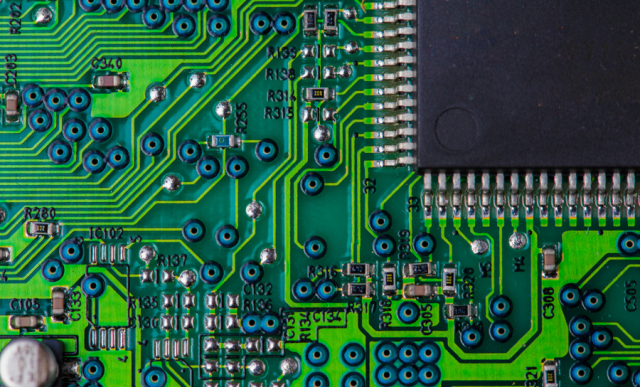
Material Characteristics of Low Dissipation Factor PCB
Low Dissipation Factor PCB laminates are typically based on advanced PTFE, hydrocarbon ceramic, or modified epoxy systems. Key material properties include:
| Parameter | Typical Range | Engineering Impact |
|---|---|---|
| Dissipation Factor (Df) | 0.0009 – 0.005 | Minimizes dielectric loss |
| Dielectric Constant (Dk) | 2.2 – 3.5 | Supports controlled impedance |
| Thermal Stability | High | Consistent RF performance |
| Moisture Absorption | Very Low | Prevents Df drift |
| Frequency Stability | Excellent | Reliable wideband behavior |
These characteristics make Low Dissipation Factor PCB materials ideal for precision RF routing and high-speed signal layers.
Low Dissipation Factor PCB vs Standard FR-4
Standard FR-4 materials typically exhibit dissipation factors around 0.015–0.020 at GHz frequencies. While acceptable for low-speed digital circuits, FR-4 introduces excessive loss in RF and high-speed designs.
Low Dissipation Factor PCB materials reduce loss by up to 70–90%, enabling:
-
Longer RF trace lengths without amplification
-
Cleaner signal transitions in high-speed digital interfaces
-
Improved efficiency in power-sensitive systems
For applications beyond a few gigahertz, Low Dissipation Factor PCB is no longer a premium option—it is a functional necessity.
Applications That Depend on Low Dissipation Factor PCB
Low Dissipation Factor PCB technology is widely adopted in performance-critical industries:
-
RF transceiver modules
-
5G and 6G base stations
-
Satellite communication payloads
-
Radar and aerospace systems
-
High-speed networking and data centers
-
Microwave backhaul and antenna feeds
In these environments, even small improvements in dielectric loss significantly enhance system-level performance.
Stackup and Layout Considerations for Low Dissipation Factor PCB
To fully leverage Low Dissipation Factor PCB materials, careful stackup and layout engineering is required:
-
Controlled impedance design based on frequency-specific Dk
-
Smooth copper surface treatments to minimize conductor loss
-
Optimized trace geometry for RF and high-speed routing
-
Proper ground reference and isolation strategies
-
Thermal expansion matching in multilayer constructions
Material selection alone is not sufficient—manufacturing precision and design discipline are equally critical.
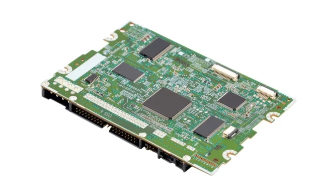
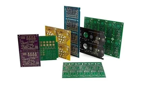
KKPCB Expertise in Low Dissipation Factor PCB Manufacturing
KKPCB specializes in engineering-driven Low Dissipation Factor PCB solutions, combining advanced materials with controlled fabrication processes:
-
Support for PTFE, Rogers, Taconic, and hybrid laminates
-
Precision impedance control for RF and high-speed designs
-
Multilayer low-loss stackups with mixed dielectric systems
-
Loss modeling and Df validation across target frequencies
-
Consistent quality for prototypes and volume production
Our Low Dissipation Factor PCB capabilities are optimized for applications where signal loss, thermal stability, and electrical predictability are non-negotiable.
Engineering Summary
Low Dissipation Factor PCB materials are a cornerstone of modern high-frequency and high-speed electronics. By minimizing dielectric loss, they enable superior signal integrity, improved power efficiency, and stable performance across demanding operating conditions.
For RF, microwave, satellite, and next-generation communication systems, Low Dissipation Factor PCB is essential to achieving predictable, scalable, and reliable designs. Through advanced material selection and precision manufacturing, KKPCB delivers Low Dissipation Factor PCB solutions that meet the highest engineering standards.
