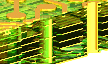
A Multilayer PCB is a printed circuit board composed of three or more conductive copper layers laminated together with insulating dielectric materials. Compared to single-layer and double-layer boards, multilayer PCBs offer higher routing density, improved electrical performance, and greater design flexibility, making them essential for modern electronic products.
As electronic systems continue to evolve toward miniaturization, higher speeds, and greater functionality, multilayer PCB technology has become a core solution for applications such as high-speed communication, RF systems, automotive electronics, industrial control, and semiconductor testing.
Key Advantages of Multilayer PCBs
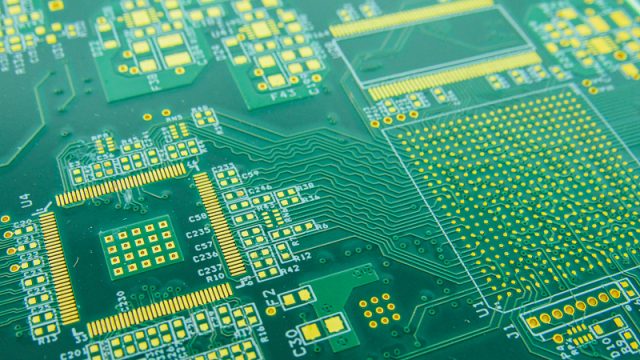
1. High-Density Circuit Integration
By stacking multiple signal, power, and ground layers, multilayer PCBs enable compact layouts and support fine-pitch components, BGAs, and high pin-count devices without increasing board size.
2. Improved Signal Integrity
Dedicated power and ground planes reduce noise, crosstalk, and EMI, while controlled impedance routing ensures stable signal transmission for high-speed and high-frequency signals.
3. Support for Controlled Impedance Designs
Multilayer PCBs allow precise control of trace geometry, dielectric thickness, and reference planes, which is critical for RF PCB, high-speed digital PCB, and 5G PCB applications.
4. Enhanced Reliability and Mechanical Stability
The laminated structure improves mechanical strength, thermal stability, and vibration resistance, making multilayer PCBs suitable for automotive, aerospace, and industrial environments.
5. Compatibility with Advanced PCB Technologies
Multilayer PCBs can be combined with HDI PCB, microvia PCB, blind and buried vias, low-loss materials, and thermal management solutions, enabling complex and high-performance designs.
Typical Multilayer PCB Stackups
Multilayer PCBs are commonly manufactured in configurations such as:
-
4-layer and 6-layer PCBs for industrial and communication equipment
-
8–12 layer PCBs for high-speed, RF, and networking systems
-
16+ layer PCBs for advanced computing, ATE, and semiconductor testing applications
Each stackup is carefully designed to balance signal integrity, power distribution, EMI control, and manufacturability.
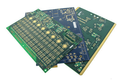
Applications of Multilayer PCBs
Multilayer PCBs are widely used across multiple industries:
-
High-speed communication and networking equipment
-
RF, microwave, and 5G systems
-
Automotive electronics, ADAS, and radar modules
-
Industrial automation and control systems
-
Medical electronics and instrumentation
-
Semiconductor IC testing, ATE, load boards, and probe cards
-
IoT devices and embedded systems
Manufacturing Considerations
Producing high-quality multilayer PCBs requires advanced fabrication and strict process control, including:
-
Precise layer alignment and lamination
-
Accurate drilling, via plating, and microvia processing
-
Controlled etching and copper thickness uniformity
-
Impedance testing and electrical reliability verification
-
Comprehensive AOI, X-ray inspection, and final testing
These processes ensure consistent performance from prototype to mass production.
Conclusion
A Multilayer PCB is the foundation of modern high-performance electronics, enabling high-density integration, excellent signal integrity, and reliable operation in complex systems. Whether for high-speed digital circuits, RF and 5G communication, automotive electronics, or semiconductor testing, multilayer PCBs provide the flexibility and performance required by today’s advanced applications.
Choosing an experienced multilayer PCB manufacturer is critical to ensuring quality, reliability, and long-term product success.
