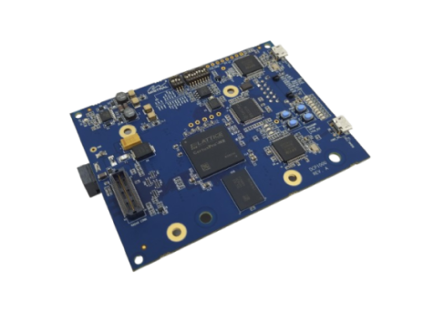
What Is an mmWave Module PCB?
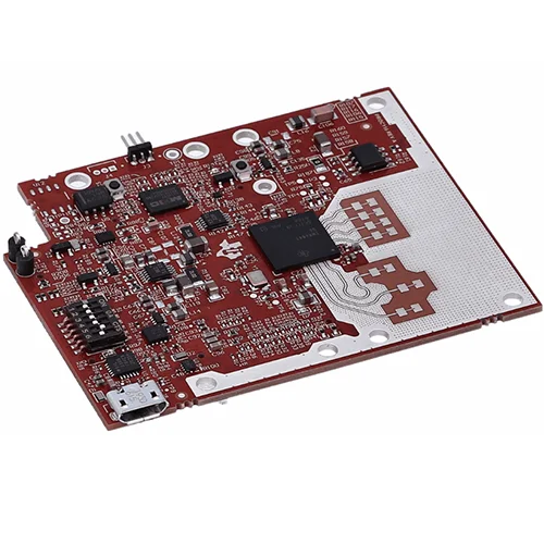
An mmWave Module PCB is a high frequency printed circuit board specifically designed for millimeter-wave applications (30–300 GHz), including:
-
5G communication modules
-
Automotive radar systems
-
High frequency IoT devices
-
Satellite communication modules
mmWave Module PCB ensures low signal loss, precise impedance control, and stable RF performance for high frequency data transmission.
Key Design Requirements
1. Low Loss High Frequency Material
mmWave signals are highly sensitive to dielectric loss. Common PCB materials for mmWave modules include:
-
RO4350B and RO4003C (Rogers)
-
RF-35 (Taconic)
-
High TG FR-4 for supporting layers
These materials provide stable dielectric constant (Dk), low dissipation factor (Df), and low insertion loss for GHz-level signals.
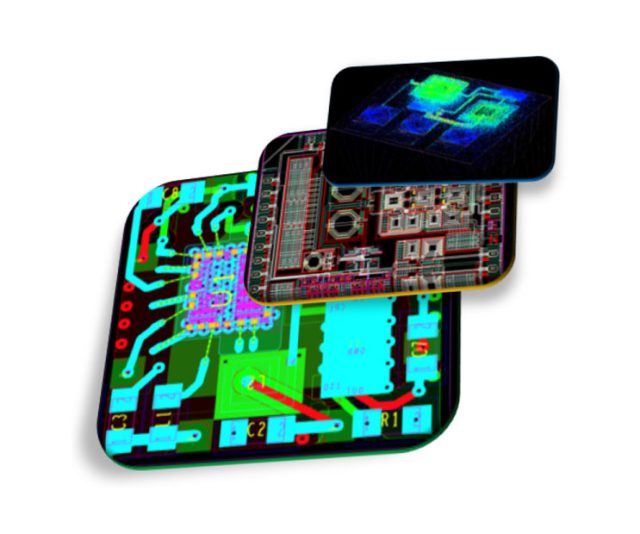
2. Controlled Impedance and Signal Integrity
Precise impedance control is critical to prevent:
-
Signal reflection
-
Crosstalk
-
Power loss
-
Data corruption
High frequency trace design includes microstrip, stripline, differential pairs, and matched length routing to maintain integrity across the mmWave band.
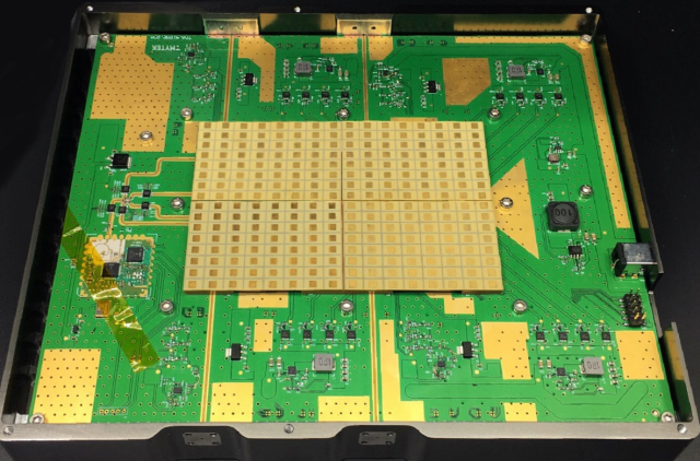
3. High Layer Count and HDI Stack-Up
mmWave modules often integrate multiple RF circuits, baseband processors, and antennas. PCB design features may include:
-
6–20 layer HDI stack-up
-
Blind and buried vias
-
Fine line and fine pitch routing
-
High pin count BGA and RF connectors
This enables compact modules without sacrificing performance.
4. Thermal and Mechanical Reliability
High frequency mmWave components generate significant heat and require mechanical stability. PCB considerations include:
-
Thermal vias and copper planes
-
Reinforced substrate for warpage prevention
-
Vibration and shock resistance for automotive or industrial applications
Applications of mmWave Module PCB
mmWave Module PCB is widely used in:
-
5G base station modules and CPE devices
-
Automotive 77GHz radar and ADAS modules
-
Satellite and aerospace communication devices
-
High frequency IoT sensor modules
-
mmWave test and measurement boards
These applications demand high signal integrity, low loss, and precise multilayer design.
mmWave Module PCB vs Standard RF PCB
| Feature | mmWave Module PCB | Standard RF PCB |
|---|---|---|
| Frequency Range | 30–300 GHz | <10 GHz |
| Material | Low loss RF laminate | Standard FR-4 or PTFE |
| Impedance Control | Critical | Moderate |
| Trace Size | Fine line / microstrip | Wider traces |
| Manufacturing Complexity | High | Moderate |
mmWave Module PCB requires more advanced design, precise fabrication, and strict quality control.
Manufacturing Considerations
Producing a high-quality mmWave Module PCB requires:
-
Tight impedance and trace width tolerance
-
Accurate multilayer lamination
-
Controlled via depth for blind/buried vias
-
Electrical testing and high frequency verification
-
Experienced manufacturer capable of GHz/mmWave PCB fabrication
Conclusion
mmWave Module PCB is a critical component in 5G, automotive radar, and high frequency IoT systems. With low loss materials, precise impedance control, and HDI multilayer stack-ups, it ensures high performance, reliable signal integrity, and compact module integration.
Choosing a professional mmWave PCB manufacturer ensures optimized stack-up, consistent electrical performance, and reliable long-term operation for advanced mmWave applications.
