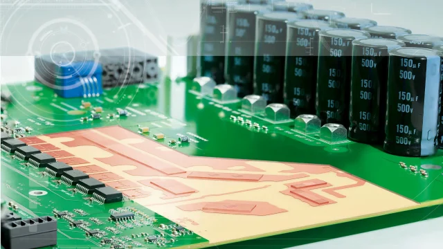
As modern electronic systems continue to operate at higher frequencies and faster data rates, signal integrity has become a critical factor in PCB design. Low Loss PCB technology is specifically developed to reduce signal attenuation and maintain high signal quality in high-speed digital and RF applications.
Low loss PCBs use specialized dielectric materials that minimize signal degradation during transmission. These circuit boards are commonly used in high-speed communication equipment, networking hardware, radar systems, and advanced computing platforms.
What Is a Low Loss PCB?
A Low Loss PCB is a printed circuit board manufactured with dielectric materials that have a low dissipation factor (Df) and stable dielectric constant. These materials significantly reduce signal loss when transmitting high-frequency or high-speed signals.
Compared with standard FR-4 materials, low loss PCB materials provide superior electrical performance, especially in applications operating at GHz frequencies.
Common low-loss PCB materials are produced by companies such as Rogers Corporation and other advanced laminate manufacturers.
Advantages of Low Loss PCB
1. Reduced Signal Attenuation
Low loss PCB materials minimize signal degradation during transmission, ensuring high signal quality over long trace lengths.
2. Improved Signal Integrity
Stable dielectric properties help maintain accurate impedance control and reduce distortion in high-speed circuits.
3. Better High-Frequency Performance
Low loss PCBs are optimized for microwave, RF, and high-speed digital systems operating at GHz frequencies.
4. Lower Power Consumption
Reduced signal loss means less energy is wasted, improving overall system efficiency.
5. Reliable High-Speed Data Transmission
Low loss PCBs support modern high-speed interfaces such as Ethernet, PCIe, and high-speed RF communication.
Design Considerations for Low Loss PCB
Designing a Low Loss PCB requires careful attention to both material selection and layout design:
-
Choosing suitable low-loss laminate materials
-
Maintaining controlled impedance for high-speed signals
-
Minimizing trace length and unnecessary vias
-
Using smooth copper surfaces to reduce conductor loss
-
Proper grounding and shielding to reduce electromagnetic interference
These design strategies help maintain optimal signal performance in high-speed circuits.
Applications of Low Loss PCB
Low loss PCBs are widely used in advanced electronic systems, including:
-
High-speed networking equipment
-
5G communication infrastructure
-
RF and microwave circuits
-
Data centers and servers
-
Satellite communication systems
-
High-performance computing devices
These applications require minimal signal loss and high signal integrity.
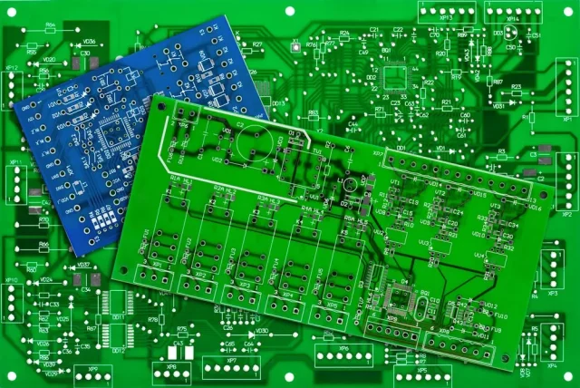
Manufacturing Requirements
Manufacturing low loss PCBs requires advanced PCB fabrication processes to maintain material integrity and electrical performance. Key factors include:
-
Precise multilayer PCB stack-up design
-
Controlled impedance manufacturing processes
-
High-quality copper foil with low surface roughness
-
Advanced surface finishes such as ENIG or immersion silver
These techniques help ensure reliable performance in high-speed electronic systems.
Conclusion
Low Loss PCB technology plays a vital role in modern high-speed and RF electronic systems. By using specialized materials and optimized PCB design techniques, low loss PCBs enable reliable high-frequency signal transmission with minimal attenuation. As communication technologies continue to evolve, low loss PCBs will remain essential for supporting next-generation high-speed electronics.
