What Is a High Frequency Signal PCB?

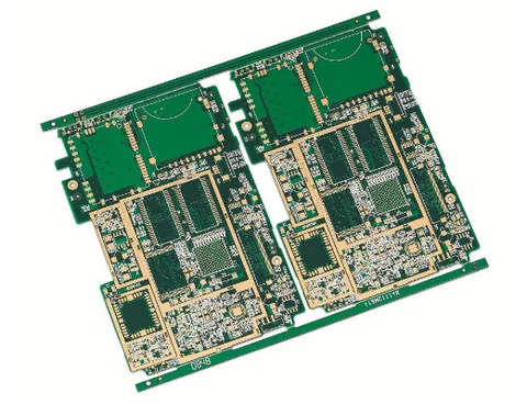
A High Frequency Signal PCB is a printed circuit board designed to transmit high-frequency electrical signals—typically in the MHz to GHz range—while maintaining signal integrity, minimizing loss, and reducing EMI. These PCBs are critical in applications such as RF communication, microwave devices, 5G modules, radar systems, high-speed networking, and IoT devices.
Unlike standard PCBs, High Frequency Signal PCBs must account for:
-
Controlled impedance
-
Insertion loss minimization
-
Return loss management
-
Crosstalk and EMI reduction
Proper design ensures reliable high-speed performance and stable signal propagation.
Why High Frequency Signal PCB Design Matters
High-frequency signals are sensitive to PCB layout, material properties, and manufacturing tolerances. Poor design can lead to:
-
Increased insertion loss and signal attenuation
-
Reflection and impedance mismatch
-
Crosstalk and noise coupling
-
EMI radiation and regulatory non-compliance
-
Reduced system performance and reliability
High Frequency Signal PCB design focuses on ensuring consistent signal integrity, low loss, and EMI control to meet stringent performance requirements.
Key Features of High Frequency Signal PCB

1. Controlled Impedance Traces
Controlled impedance routing is critical for high-frequency signals. Typical impedance values include:
-
50Ω single-ended for RF traces
-
75Ω traces for video/RF applications
-
100Ω differential traces for high-speed data links
Consistent impedance reduces reflections and signal degradation.
2. Low Loss PCB Materials
High Frequency Signal PCBs require low-loss laminates to reduce signal attenuation at high frequencies. Common materials include:
-
Rogers RO4003C, RO4350B, RO3003
-
Duroid / PTFE-based laminates
-
Megtron series laminates for low-loss high-speed circuits
These materials maintain stable dielectric constant (Dk) and low dissipation factor (Df), improving high-frequency performance.
3. Multilayer Stack-Up Optimization
Stack-up design affects signal propagation, EMI, and return path integrity. High Frequency Signal PCBs often use:
-
Microstrip or stripline traces for controlled impedance
-
Solid ground planes under critical RF traces
-
Layer isolation to reduce crosstalk and coupling
-
Optimized via transitions to minimize signal reflections
Proper multilayer design supports both high-frequency analog and high-speed digital signals.
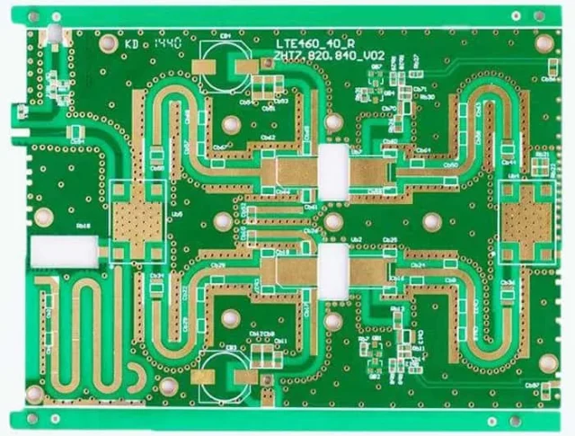
4. RF Trace Geometry and Layout
High Frequency Signal PCB layout follows specific geometry rules:
-
Smooth trace bends and consistent width
-
Minimal discontinuities at vias and layer transitions
-
Proper spacing between high-frequency traces
-
Short and direct routing to minimize loss
Good trace geometry improves insertion loss and reduces radiation.
5. EMI Control and Grounding
High-frequency circuits generate EMI, which must be managed through:
-
Continuous reference planes for return currents
-
Via stitching for grounding and shielding
-
Ground fences or guard traces around sensitive signals
-
Separation of noisy digital and analog sections
This ensures EMC compliance and signal integrity.
Common Applications of High Frequency Signal PCBs

High Frequency Signal PCBs are used in:
-
5G and wireless communication modules
-
WiFi, Bluetooth, and IoT RF modules
-
GPS navigation and positioning systems
-
Automotive radar and ADAS systems
-
Microwave and satellite communication systems
-
High-speed networking and server backplanes
-
High-speed digital logic boards with sensitive RF signals
-
IC test PCBs for high-frequency characterization
KKPCB High Frequency Signal PCB Manufacturing Capabilities
KKPCB offers professional High Frequency Signal PCB manufacturing with advanced engineering support, including:
-
Low-loss and high-frequency laminate PCB fabrication
-
Controlled impedance and differential pair routing
-
Fine line PCB and HDI PCB manufacturing for compact designs
-
Optimized multilayer stack-ups for RF and high-speed circuits
-
Via backdrill and microvia processing for reduced reflection
-
High-reliability production and strict quality inspection
-
Prototype to mass production support
Our expertise ensures High Frequency Signal PCBs maintain low-loss, high signal integrity, and reliable high-speed performance.
Conclusion
A High Frequency Signal PCB is essential for modern RF, microwave, 5G, and high-speed digital applications. By carefully selecting low-loss materials, optimizing stack-up, controlling impedance, and managing EMI, High Frequency Signal PCBs achieve reliable signal transmission and high system performance.
KKPCB delivers high-quality High Frequency Signal PCB solutions with advanced manufacturing, precise engineering support, and consistent production reliability.

