What Is a High Frequency Signal PCB?
A High Frequency Signal PCB is a printed circuit board designed to carry high-speed and high-frequency signals with minimal loss, reflection, or distortion. These PCBs are crucial in RF, microwave, 5G, high-speed computing, and semiconductor test applications, where signal integrity and low insertion loss are essential for system performance.
Why High Frequency Signal PCB Technology Matters
As electronic systems operate at gigahertz frequencies, traditional PCB designs struggle to maintain signal quality. High frequency signal PCBs address challenges such as:
-
Signal attenuation over long traces
-
Impedance mismatch and reflections
-
Crosstalk and electromagnetic interference (EMI)
-
Dielectric and conductor losses
-
Phase instability and signal distortion
They ensure stable, high-speed signal propagation in demanding applications.
Key Features of High Frequency Signal PCBs
High-quality high frequency signal PCBs include:
-
Controlled impedance traces for consistent signal transmission
-
Low-loss dielectric materials to minimize insertion loss
-
Precision microvia and fine line routing
-
Optimized layer stackup for signal integrity
-
Shielding and ground plane optimization
These features maintain signal fidelity and high-speed performance.
Design Considerations for High Frequency Signal PCBs
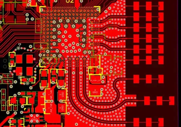
Designing high frequency signal PCBs requires:
-
Trace width and spacing calculation for controlled impedance
-
Minimizing via stubs and discontinuities
-
Crosstalk reduction through layer assignment and shielding
-
Differential pair routing for high-speed interfaces
-
Fan-out optimization for fine-pitch ICs
Careful design ensures low jitter, minimal signal loss, and high data integrity.
Materials for High Frequency Signal PCBs
Material selection is crucial for high frequency applications:
-
Low-loss laminates such as Rogers RO4003C, RO4350B, Duroid 5880/6010, Taconic RF-35
-
High-TG FR-4 for hybrid high-speed boards
-
Smooth copper foils to reduce conductor loss
-
Polyimide or composite materials for flexible RF layouts
Proper materials ensure stable signal propagation and minimal insertion loss.
Manufacturing Capabilities for High Frequency Signal PCBs
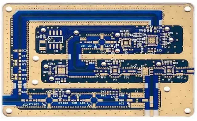
Producing high frequency signal PCBs requires:
-
Precision etching and microvia drilling
-
Tight layer-to-layer registration
-
Controlled impedance verification (TDR testing)
-
Multilayer HDI stackup capability
-
Automated optical inspection (AOI) and electrical testing
Professional manufacturing guarantees consistent high-frequency performance and reliability.
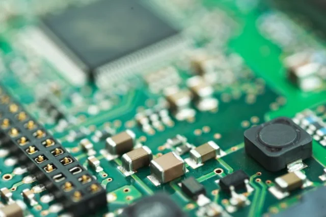
Assembly Considerations for High Frequency Signal PCBs
Assembly includes:
-
Fine-pitch component placement and soldering
-
Preserving differential pairs and high-speed nets
-
Shielding integration for EMI reduction
-
Functional testing for RF signal quality
-
ESD-safe handling for sensitive components
Proper assembly ensures signal integrity and long-term reliability.
Applications of High Frequency Signal PCBs
High frequency signal PCBs are widely used in:
-
5G and mmWave communication modules
-
RF transceivers and wireless systems
-
High-speed computing and data acquisition boards
-
Semiconductor test boards and ATE systems
-
Automotive radar and ADAS electronics
-
Aerospace, satellite, and defense RF modules
They are essential wherever high-frequency, low-loss signal transmission is required.
Why Choose a Professional High Frequency Signal PCB Manufacturer
A professional manufacturer provides:
-
Expertise in high-frequency PCB design and controlled impedance
-
Material selection for low-loss, stable signal propagation
-
Prototype, small batch, and mass production support
-
Advanced inspection, TDR testing, and functional validation
-
One-stop PCB fabrication and assembly services
The right partner ensures high-frequency performance, signal integrity, and reliable system operation.
