High-frequency electronics are rapidly expanding across modern industries. From 5G communication infrastructure and WiFi systems to radar sensing, satellite communication, and advanced RF front-end modules, more products are operating in the GHz range than ever before. In these designs, the PCB is not just a carrier for components—it becomes a critical part of the signal path.
A High Frequency Signal PCB is specifically engineered to transmit high-frequency signals with low insertion loss, stable controlled impedance, and strong EMI suppression. Compared with standard digital PCB designs, high-frequency signal routing is far more sensitive to material properties, stack-up accuracy, trace geometry, and via transitions. Even small deviations can cause impedance discontinuities, signal reflections, and degraded RF performance.
This article introduces what a High Frequency Signal PCB is, why it matters, and how to design and manufacture high frequency PCBs for stable, reliable GHz-level performance.
What Is a High Frequency Signal PCB?
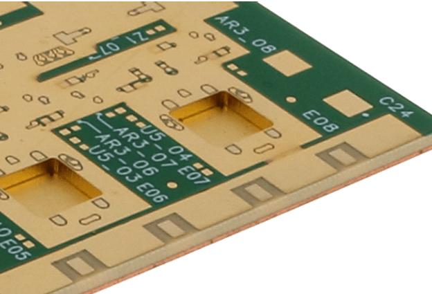
A High Frequency Signal PCB is a printed circuit board designed to support signal transmission at high frequencies, typically in the hundreds of MHz to multiple GHz range. At these frequencies, traces behave as transmission lines rather than simple conductors. This means the PCB must be designed and manufactured with strict control over impedance, dielectric properties, and signal return paths.
A typical High Frequency Signal PCB includes:
-
Controlled impedance RF traces (50Ω, 75Ω, or application-specific values)
-
Transmission line routing such as microstrip and stripline
-
Low-loss dielectric materials to reduce attenuation
-
Solid reference planes for stable return current paths
-
EMI control structures such as ground vias and shielding fences
High Frequency Signal PCBs are widely used in RF and microwave circuits where stable signal quality and low loss are essential.
Why High Frequency Signal PCB Performance Is So Important
1. High Frequency Signals Are Extremely Sensitive to Loss
At GHz frequencies, signal loss becomes one of the biggest design limitations. Loss can come from dielectric loss, conductor loss, surface roughness effects, and discontinuities in routing.
A High Frequency Signal PCB is designed to reduce loss by:
-
Using low loss PCB materials with low dissipation factor (Df)
-
Optimizing trace geometry and routing length
-
Selecting suitable copper and surface finishes
-
Minimizing unnecessary via transitions and stubs
Lower insertion loss helps maintain signal amplitude and improves receiver sensitivity, which is critical in RF systems.
2. Controlled Impedance PCB Design Prevents Reflections
Impedance control is a core requirement for every High Frequency Signal PCB. When impedance changes along a trace due to geometry variation or stack-up inconsistency, reflections occur. Reflections can cause return loss issues, signal distortion, and unstable RF behavior.
High Frequency Signal PCBs typically require:
-
Accurate trace width control
-
Stable dielectric thickness and Dk consistency
-
Clean reference plane design
-
Controlled impedance testing during production
A stable controlled impedance PCB ensures reliable signal transfer from source to load.
3. EMI and Crosstalk Risks Increase at High Frequency
High-frequency signals can radiate more easily and are more susceptible to interference. Poor layout, weak grounding, and improper isolation can cause EMI issues that degrade system performance or cause compliance failures.
High Frequency Signal PCB designs often include:
-
Ground via stitching near RF traces
-
Isolation gaps and keep-out zones
-
Proper spacing between RF and digital signals
-
Shielding techniques for sensitive RF sections
These methods help reduce EMI and improve signal stability.
High Frequency Signal PCB Materials: Rogers, PTFE, and Low Loss Laminates
Material selection is one of the most important decisions in high frequency PCB design. Standard FR-4 may work for low-frequency circuits, but it often introduces excessive loss at GHz frequencies.
Common High Frequency Signal PCB material options include:
Rogers PCB Materials
Rogers laminates are widely used in high-frequency applications due to stable Dk and low loss performance. Popular options include:
-
RO4003C PCB for high frequency and controlled impedance designs
-
RO3003 PCB for ultra-low loss and high-frequency stability
Rogers PCB materials are commonly used in 5G, radar, and RF front-end circuits.
PTFE and Duroid PCB Materials
PTFE-based materials, including Duroid PCB laminates, provide extremely low loss and excellent performance at microwave frequencies.
They are often used for:
-
Microwave amplifiers
-
High-performance antennas
-
Satellite communication modules
-
Radar and sensing systems
PTFE PCB and Duroid PCB materials are excellent for high frequency signal transmission but require specialized fabrication processes.
Hybrid High Frequency Signal PCB Stack-Ups
Many projects combine high-frequency materials with FR-4 in a hybrid stack-up to balance performance and cost. Hybrid High Frequency Signal PCBs are common when only certain layers require low-loss routing.
Hybrid stack-ups can support:
-
RF layers using Rogers or PTFE
-
Digital control layers using FR-4
-
Power distribution layers for system integration
This approach improves performance while keeping the overall PCB cost reasonable.
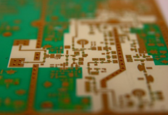
High Frequency Signal PCB Routing: Microstrip vs Stripline
High Frequency Signal PCBs use transmission line structures designed for stable impedance control.
Microstrip Routing
Microstrip traces are routed on outer layers with a reference plane beneath. They are easy to tune and commonly used for antenna feeds and RF component routing.
Advantages:
-
Easy measurement and adjustment
-
Suitable for RF front-end layouts
-
Practical for many high frequency PCB applications
Stripline Routing
Stripline traces are routed on inner layers between two reference planes. This provides better shielding and lower EMI radiation.
Advantages:
-
Better EMI containment
-
More stable impedance environment
-
Higher isolation in dense layouts
Stripline is widely used in multilayer High Frequency Signal PCB designs where interference control is critical.
Manufacturing Requirements for High Frequency Signal PCB Fabrication
High Frequency Signal PCB manufacturing requires tight process control to ensure repeatable electrical performance. Even small variations can impact impedance and RF behavior.
Key manufacturing considerations include:
1. Stack-Up Control and Dielectric Thickness Accuracy
Precise lamination control ensures stable impedance and consistent RF performance across batches.
2. High Precision Etching for Trace Width Control
Accurate line width and spacing are critical for controlled impedance PCB production.
3. Controlled Impedance Testing
High frequency PCBs often require impedance verification to confirm 50Ω/75Ω trace performance.
4. Via Design and Transition Quality
Vias can introduce discontinuities at high frequency. Manufacturers must ensure clean drilling, plating, and proper via structures.
5. Surface Finish Selection
Surface finish impacts RF loss and assembly performance. Suitable finishes can help improve high-frequency signal transmission.
Best Practices for High Frequency Signal PCB Design
To improve High Frequency Signal PCB performance, engineers commonly follow these design rules:
-
Keep high frequency traces short and direct
-
Avoid sharp corners; use smooth bends
-
Maintain continuous reference planes under RF traces
-
Add ground via stitching near RF traces and connectors
-
Avoid routing RF signals near noisy power circuits
-
Reduce via count and minimize via stubs
-
Use proper RF connector launch design
-
Validate design with simulation when needed
These best practices help reduce reflections, improve insertion loss performance, and maintain stable signal integrity.
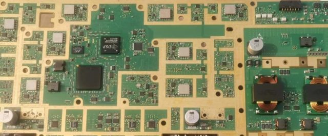
Applications of High Frequency Signal PCBs
High Frequency Signal PCBs are used across many industries, including:
-
5G communication systems
-
Wireless communication modules
-
Antenna and RF front-end products
-
Radar sensors and automotive radar
-
Satellite communication equipment
-
Microwave amplifiers and filters
-
IoT and GPS devices
-
Aerospace and defense RF systems
In each of these applications, stable controlled impedance and low loss are essential for reliable operation.
Conclusion: Why Choose a High Frequency Signal PCB?
A High Frequency Signal PCB is essential for any design operating at GHz frequencies where signal loss, impedance stability, and EMI control are critical. By combining low loss materials, controlled impedance routing, optimized stack-up design, and precise PCB fabrication processes, high frequency PCBs provide reliable performance for advanced RF and microwave applications.
If your project requires a High Frequency PCB with controlled impedance, low insertion loss, and high reliability, choosing the right material system and an experienced manufacturer is the key to achieving consistent results.
