What Actually Defines an HDI PCB?
An HDI PCB (High-Density Interconnect PCB) is not defined by layer count alone, but by how efficiently interconnections are implemented. The key differentiators are:
- Microvias (laser-drilled vias)
- Blind and buried vias
- Fine line and spacing (typically ≤100 µm)
- High connection density per unit area
The goal of HDI is simple but powerful:
Increase routing efficiency without increasing board size
Instead of adding more layers like traditional multilayer PCBs, HDI improves how each layer is used.
Stack-Up Choices: 1+N+1 vs 2+N+2
One of the most critical decisions in HDI design is selecting the right stack-up structure.
1+N+1 Structure:
- One buildup layer on each side of the core
- Lower cost and complexity
- Suitable for moderate-density designs
2+N+2 Structure:
- Two buildup layers on each side
- Supports higher routing density and finer pitch components
- Higher cost due to additional lamination cycles
Key Insight:
Choosing a higher stack-up is not always better. The optimal structure depends on:
- BGA pitch
- Routing congestion
- Signal speed requirements
- Cost constraints
A well-optimized 1+N+1 design can often replace an unnecessarily complex 2+N+2 stack-up.
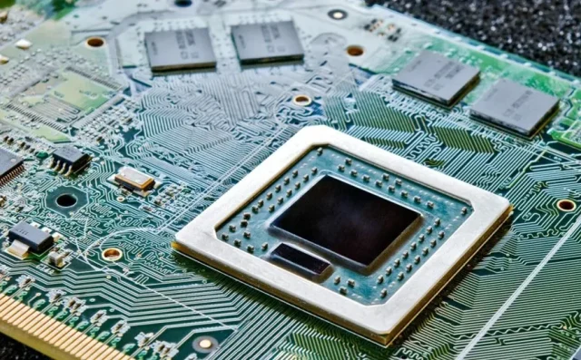
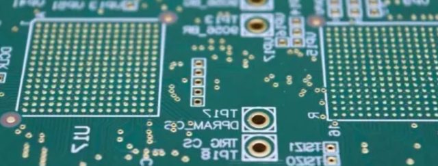
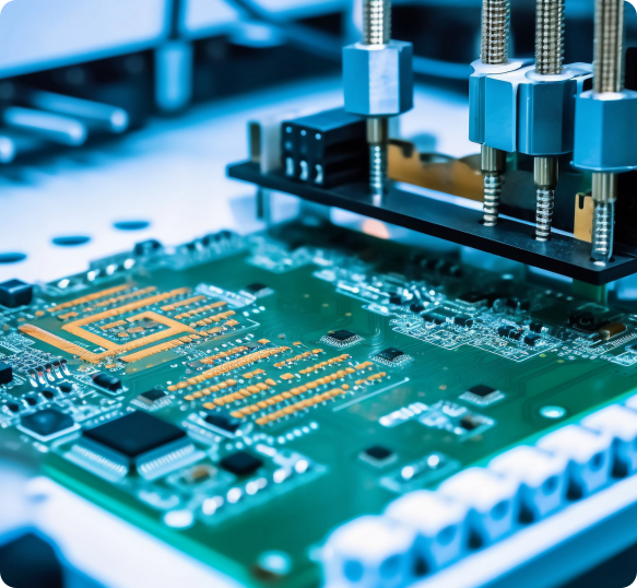
Via Strategy: The Core of HDI
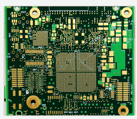
In HDI PCBs, vias are not just connections—they define the entire routing capability.
- Microvias:
Short interconnects that reduce signal path length and improve performance - Stacked Microvias:
Enable vertical routing but require strict process control - Staggered Microvias:
Improve reliability and are easier to manufacture - Via-in-Pad:
Essential for fine-pitch BGAs, allowing direct escape routing - Blind/Buried Vias:
Used to optimize internal layer connections without consuming outer-layer space
Engineering Trade-Off:
- Stacked vias → higher density, higher risk/cost
- Staggered vias → better reliability, slightly more routing complexity
Cost Drivers You Can’t Ignore
HDI is powerful—but it comes at a cost. Understanding cost drivers helps avoid overdesign.
Key factors affecting cost:
- Number of lamination cycles
- Microvia count and complexity
- Fine line processing requirements
- Material selection (standard vs high-speed)
- Yield impact from dense structures
A common mistake is overusing HDI features where they are not necessary.
Smart HDI design = minimum complexity for required performance
Design Decision Workflow (Practical Guide)
Instead of asking “Should I use HDI?”, engineers should follow a structured approach:
- Check Component Requirements
- BGA pitch ≤0.8 mm? → Consider HDI
- ≤0.5 mm? → HDI is likely required
- Evaluate Routing Density
- Routing congestion on standard multilayer? → HDI can help
- Assess Signal Performance Needs
- High-speed (DDR, PCIe, SerDes)? → HDI improves SI
- Select Stack-Up
- Start with 1+N+1 → increase only if necessary
- Optimize Via Strategy
- Prefer staggered vias unless density demands stacking
- Balance Cost vs Performance
- Avoid overdesigning beyond actual requirements
This workflow helps ensure the design is efficient, manufacturable, and cost-effective.
Final Thoughts
HDI PCBs are not just about miniaturization—they are about engineering smarter interconnect systems.
The real value of HDI lies in:
- Efficient routing
- Improved signal performance
- Reduced form factor
- Scalable design architecture
At KKPCB, we work closely with customers to optimize HDI stack-ups, via strategies, and manufacturability, ensuring designs achieve the right balance between performance, reliability, and cost.
