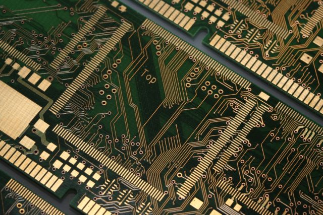
An HDI PCB (High Density Interconnect PCB) is a key technology enabling compact, lightweight, and high-performance electronic products. As electronic devices continue to evolve toward smaller form factors, higher functionality, and faster data transmission, traditional PCB designs can no longer meet density and routing requirements.
HDI PCB technology provides higher wiring density per unit area by using microvias, fine line and space, and multilayer structures, making it essential for advanced electronic applications.
What Is an HDI PCB?
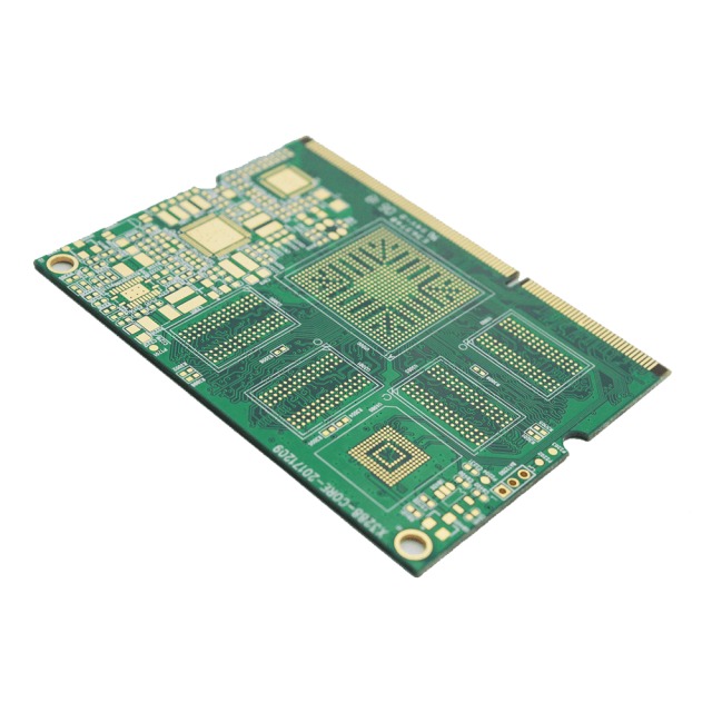
An HDI PCB is a printed circuit board that features higher circuit density compared to conventional PCBs. This is achieved through the use of:
-
Microvias (laser-drilled vias)
-
Blind and buried vias
-
Fine line and space routing
-
High layer count with compact stack-ups
HDI PCBs allow designers to route more signals in less space while maintaining signal integrity and reliability.
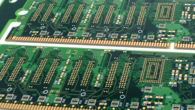
Key Features of HDI PCB Technology
Microvia Interconnection
Microvias enable direct layer-to-layer connections, reducing signal path length and improving electrical performance.
Fine Line and Space
HDI PCB manufacturing supports extremely fine trace widths and spacing, allowing higher routing density.
Compact Multilayer Structures
HDI PCBs support complex multilayer designs while maintaining thin board thickness.
Improved Signal Integrity
Shorter interconnect paths reduce signal loss, crosstalk, and electromagnetic interference.
Advantages of Using HDI PCBs
Choosing an HDI PCB offers several important benefits:
-
Reduced PCB size and weight
-
Higher component density
-
Enhanced electrical performance
-
Improved thermal management
-
Better reliability for high-speed designs
-
Increased design flexibility
These advantages make HDI PCBs ideal for next-generation electronic systems.
HDI PCB Manufacturing Capabilities
Producing a reliable HDI PCB requires advanced manufacturing technologies and strict process control:
-
Laser drilling for microvias
-
Sequential lamination processes
-
Fine line etching with tight tolerance
-
Blind and buried via fabrication
-
Controlled impedance PCB processing
-
Advanced AOI and electrical testing
An experienced HDI PCB manufacturer ensures consistent quality and high yield.
Materials Used in HDI PCB Manufacturing
HDI PCBs can be manufactured using various materials depending on application requirements:
-
High-Tg FR-4 for standard HDI designs
-
Low-loss materials for high-speed and RF HDI PCBs
-
Hybrid stack-ups for mixed-signal applications
Material selection affects signal integrity, thermal performance, and long-term reliability.
Design Considerations for HDI PCBs
Successful HDI PCB design requires careful planning and collaboration with the manufacturer:
-
Stack-up optimization for microvia structures
-
Via-in-pad design and filling processes
-
Signal integrity and impedance control
-
Power and ground plane design
-
Thermal and mechanical reliability
Early DFM review helps reduce design iterations and manufacturing risks.
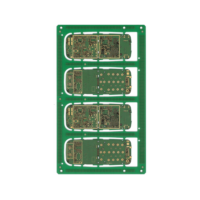
Applications of HDI PCBs
HDI PCBs are widely used in:
-
Smartphones and wearable electronics
-
5G communication modules
-
High-speed computing and servers
-
Automotive electronics and ADAS systems
-
Medical devices
-
Semiconductor test and ATE systems
In these applications, HDI PCBs enable high performance within compact designs.
HDI PCB from Prototype to Mass Production
HDI PCB projects often begin with prototype development to validate routing density, signal performance, and manufacturability. Once verified, designs are scaled to mass production using consistent materials and controlled processes.
Working with a qualified HDI PCB supplier ensures stable quality and reliable delivery throughout the product lifecycle.
Conclusion
An HDI PCB is a foundational technology for modern high-performance electronic designs. By enabling higher interconnection density, improved signal integrity, and compact form factors, HDI PCBs support the continued advancement of electronic products across multiple industries.
Partnering with an experienced HDI PCB manufacturer ensures precision manufacturing, engineering support, and scalable production for even the most demanding applications.
