What Is a Differential Pair PCB?
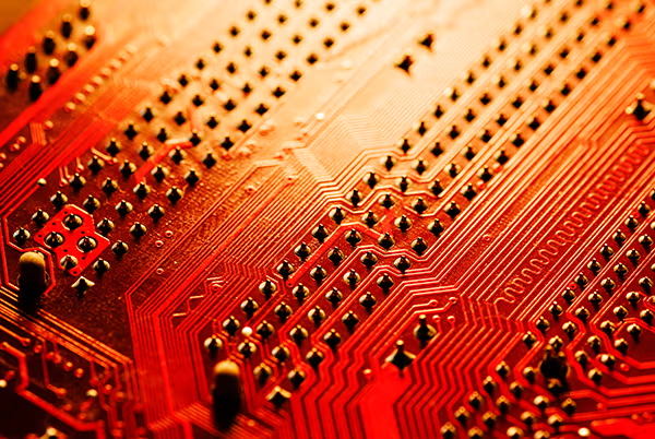
A Differential Pair PCB is a printed circuit board designed to route differential signal pairs, which are two complementary signals transmitted simultaneously to improve noise immunity, reduce crosstalk, and maintain signal integrity. Differential pair technology is critical in high-speed digital interfaces, such as USB, HDMI, PCIe, Ethernet, DDR memory, and 5G modules.
Why Differential Pair PCB Technology Matters
As data rates increase, single-ended routing often suffers from:
-
Electromagnetic interference (EMI)
-
Signal reflection due to impedance mismatch
-
Timing skew and jitter
-
Crosstalk between adjacent traces
-
Signal attenuation over long or dense routing
Differential pair PCBs maintain balanced signal propagation, enabling reliable communication in high-speed digital systems.
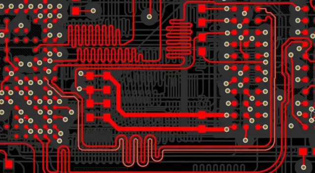
Key Features of Differential Pair PCBs
High-quality differential pair PCBs typically feature:
-
Tightly matched trace widths and spacing for consistent impedance
-
Controlled impedance and return paths
-
Optimized layer stackup for noise reduction
-
Differential pair routing with minimal vias
-
Shielding and ground plane optimization
These features ensure clean signal transmission even at gigahertz frequencies.
Design Considerations for Differential Pair PCBs
Effective differential pair PCB design requires:
-
Trace length matching to minimize timing skew
-
Maintaining constant trace separation to control impedance
-
Avoiding stubs or unnecessary vias
-
Crosstalk reduction through ground shielding
-
Layer stackup optimization for high-speed signals
Design precision ensures low jitter, minimal skew, and signal integrity.
Materials for Differential Pair PCBs
Material choice is crucial for high-speed differential signaling:
-
Low-loss laminates such as Rogers RO4003C, RO4350B, Duroid, Taconic RF-35
-
High TG FR-4 for thermal and mechanical stability
-
Smooth copper foils for low insertion loss
-
Hybrid materials for mixed-signal integration
Proper materials ensure consistent impedance and low signal distortion.
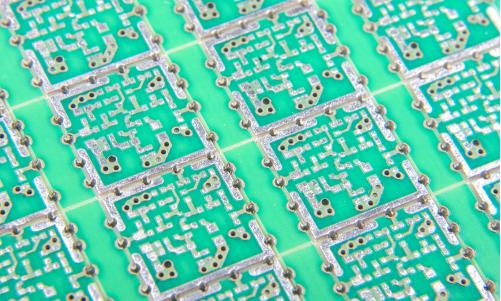
Manufacturing Capabilities for Differential Pair PCBs
Producing high-quality differential pair PCBs requires:
-
Precision etching and trace width control
-
Laser-drilled microvias for HDI and fan-out
-
Layer-to-layer registration accuracy
-
Impedance verification using TDR testing
-
Automated optical inspection (AOI) and electrical testing
Strict process control ensures high-speed differential performance.
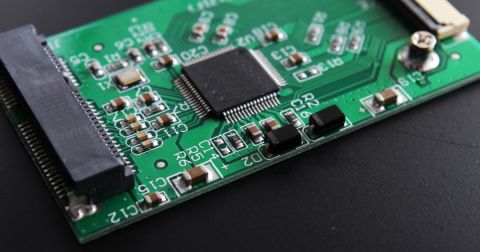
Assembly Considerations for Differential Pair PCBs
Assembly includes:
-
Fine-pitch component placement preserving differential pairs
-
Controlled soldering profiles to avoid skew or misalignment
-
Shielded connectors and routing to maintain signal quality
-
Functional high-speed testing of differential interfaces
-
ESD-safe handling for sensitive components
Correct assembly maintains signal integrity and long-term reliability.
Applications of Differential Pair PCBs
Differential pair PCBs are widely used in:
-
High-speed computing and server boards
-
Networking equipment and Ethernet interfaces
-
Memory modules (DDR, LPDDR)
-
5G and high-speed RF communication modules
-
High-speed ADC/DAC data acquisition systems
-
Automotive electronics and ADAS modules
They are essential wherever balanced, high-speed signal transmission is required.
Why Choose a Professional Differential Pair PCB Manufacturer
An experienced manufacturer provides:
-
Expertise in high-speed differential pair design
-
Controlled impedance manufacturing
-
Advanced inspection and TDR testing
-
Prototype, small batch, and mass production support
-
One-stop PCB fabrication and assembly services
The right partner ensures signal integrity, minimal jitter, and reliable high-speed performance.
