As electronic systems continue to integrate higher data rates, greater power density, and tighter form factors, high layer count PCBs have become a foundational platform for modern hardware architecture. Designs exceeding 16, 20, or even 30 layers are now common in data center equipment, telecommunications infrastructure, aerospace electronics, and industrial control systems.
However, increasing layer count does not automatically solve system complexity. Without disciplined engineering, high layer count PCB designs often introduce signal integrity degradation, unstable power delivery, and severe thermal bottlenecks. Effective high layer count PCB design must therefore be treated as a system-level engineering problem, not merely a routing exercise.
Signal Integrity Challenges in High Layer Count PCBs
High layer count PCB layouts typically support high-speed interfaces such as PCIe, Ethernet, SerDes, and RF control signals. At these data rates, interconnect behavior is dominated by electromagnetic effects rather than DC connectivity.
Key signal integrity challenges include:
-
Impedance discontinuities caused by inconsistent dielectric thickness across layers
-
Excessive via stubs in deep multilayer stackups
-
Crosstalk between densely routed differential pairs
-
Mode conversion introduced by asymmetric reference planes
To mitigate these risks, controlled impedance PCB structures must be embedded into the stackup from the earliest design phase. Dedicated reference planes, symmetric layer pairing, and back-drilled or blind/buried via strategies are essential to maintain stable signal integrity in high layer count PCB architectures.
Power Integrity and Layer Stackup Strategy
As layer count increases, power delivery networks (PDNs) become more complex. High-performance processors, FPGAs, and power modules demand low-impedance, low-inductance power paths across multiple voltage domains.
Effective high layer count PCB designs typically allocate:
-
Multiple solid power and ground plane pairs
-
Closely coupled plane spacing to reduce loop inductance
-
Distributed decoupling capacitors aligned with power plane segmentation
Poor stackup planning often leads to voltage ripple, transient droop, and electromagnetic interference. By contrast, a well-structured high layer count PCB stackup enables stable power integrity while supporting high-speed signal routing on adjacent layers.
Thermal Management in High Layer Count PCB Designs
Thermal challenges scale rapidly with layer count. Dense copper distribution, stacked power devices, and limited airflow paths can trap heat within the PCB structure.
High layer count PCB thermal management relies on:
-
Strategic copper balancing to avoid localized hotspots
-
Thermal via arrays connecting internal heat-generating layers
-
Integration of heavy copper or enhanced thermal planes where required
-
Controlled resin flow during lamination to maintain thermal consistency
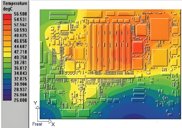
Thermal simulation at the stackup level is increasingly used to predict heat distribution before fabrication, reducing the risk of field failures in high-reliability applications.
Via Architecture and Manufacturability Considerations
Via strategy defines the mechanical and electrical feasibility of high layer count PCB fabrication. Blind vias, buried vias, and sequential lamination are commonly required to maintain routing density without compromising reliability.
Key engineering considerations include:
-
Aspect ratio control to ensure plating reliability
-
Minimization of via stub length for high-speed signals
-
Registration accuracy across multiple lamination cycles
-
Resin integrity around via barrels under thermal stress
From a manufacturing perspective, high layer count PCBs demand tight process control, advanced drilling accuracy, and rigorous electrical testing to ensure long-term performance stability.
KKPCB Engineering Approach
At KKPCB, high layer count PCB projects are managed through design-for-manufacturing (DFM) collaboration and process-driven fabrication control. Engineering reviews focus on stackup feasibility, impedance modeling, thermal risk assessment, and via reliability before production begins.
By combining controlled impedance manufacturing, precision lamination, and advanced inspection processes, KKPCB delivers high layer count PCBs that meet both electrical performance requirements and long-term reliability expectations.
Engineering Summary
High layer count PCBs are no longer niche solutions—they are a core enabler for advanced electronic systems. Successfully designing these boards requires a holistic understanding of signal integrity, power integrity, thermal behavior, and manufacturing constraints.
When approached with disciplined engineering and manufacturing expertise, high layer count PCBs provide a stable, scalable platform capable of supporting the most demanding modern applications.
For complex multilayer PCB challenges, early engineering engagement is the key to success.
