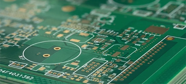
In modern PCB design, the choice and handling of substrate materials play a critical role in determining the overall performance, reliability, and manufacturability of the circuit board. Substrate-related issues can lead to serious defects such as poor solderability, delamination, signal loss, and even complete product failure.
This article outlines the most common substrate problems encountered in PCB manufacturing and provides practical inspection methods and effective solutions to improve product quality and production stability.
1. Soldering Defects Caused by Substrate Issues
Phenomenon
- Cold solder joints
- Blow holes or voids in solder joints
- Poor wetting and weak bonding strength
Root Causes
- High moisture absorption in PCB substrate materials
- Contamination or oxidation on substrate surface
- Improper storage conditions before assembly
Inspection Methods
- Pre-bake moisture analysis
- Visual inspection and X-ray analysis of solder joints
- Surface cleanliness testing
Solutions
- Use low-moisture absorption materials such as high-quality FR-4 or Rogers substrates
- Implement proper baking procedures before SMT assembly
- Store PCB boards in controlled humidity environments (≤40% RH)
- Apply surface treatments like ENIG to improve solderability
2. Delamination and Layer Separation
Phenomenon
- Separation between layers
- Blistering or bubbles on PCB surface
- Reduced mechanical strength
Root Causes
- Mismatch in thermal expansion coefficients (CTE)
- Poor lamination process control
- Excessive thermal stress during reflow soldering
Inspection Methods
- Cross-section analysis
- Thermal cycling tests
- Microsection inspection
Solutions
- Select substrates with matched CTE values
- Optimize lamination pressure, temperature, and time
- Use high Tg (glass transition temperature) materials
- Control reflow temperature profiles carefully
3. Warpage and Deformation of PCB
Phenomenon
- PCB bending or twisting
- Assembly misalignment during SMT process
- Difficulty in automated placement
Root Causes
- Uneven copper distribution
- Incorrect substrate thickness selection
- Residual stress during manufacturing
Inspection Methods
- Warpage measurement tools
- Flatness inspection before assembly
Solutions
- Optimize PCB layout with balanced copper distribution
- Choose appropriate substrate thickness
- Use symmetrical layer stack-up design
- Control cooling rate after lamination
4. Electrical Performance Degradation
Phenomenon
- Signal integrity issues
- Increased signal loss in high-frequency circuits
- Impedance instability
Root Causes
- High dielectric loss of substrate material
- Inconsistent dielectric constant (Dk)
- Poor material selection for high-speed applications
Inspection Methods
- Impedance testing
- Signal integrity simulation
- High-frequency performance testing
Solutions
- Use low-loss materials such as Rogers or PTFE substrates
- Ensure tight control of dielectric constant
- Collaborate with PCB manufacturers for material selection
- Optimize trace design for impedance control
5. CAF (Conductive Anodic Filament) Failure
Phenomenon
- Electrical short circuits between vias or traces
- Intermittent or permanent failure in humid environments
Root Causes
- Moisture ingress into substrate
- Poor resin quality or glass fiber interface
- High voltage bias under humid conditions
Inspection Methods
- CAF testing under high humidity conditions
- Insulation resistance testing
Solutions
- Use CAF-resistant substrate materials
- Improve resin formulation and glass fiber bonding
- Apply protective coatings
- Control environmental humidity during operation
Conclusion
Substrate selection and management are fundamental to achieving high-performance PCB design and reliable PCB assembly. From soldering defects to electrical performance issues, most problems can be traced back to improper material selection, poor process control, or environmental factors.
By understanding these common substrate problems and implementing the right solutions, manufacturers and designers can significantly enhance PCB reliability, reduce failure rates, and improve overall product quality.
