What Is a Buried Via PCB?
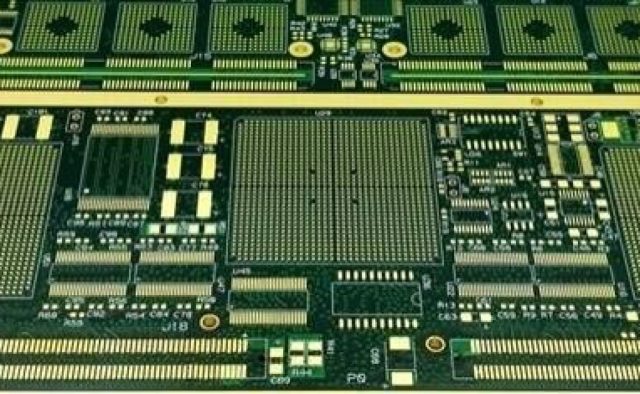
A Buried Via PCB is a multilayer printed circuit board that contains vias connecting internal layers only, without reaching the outer surface layers.
Unlike through-hole vias, buried vias are completely enclosed within the board stack-up. This allows designers to:
-
Increase routing density
-
Optimize outer layer space
-
Improve signal integrity
-
Reduce board size
Buried Via PCB technology is commonly used in HDI PCB and high layer count PCB designs.
How Buried Vias Work
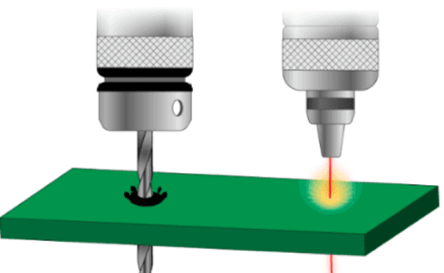
In a standard multilayer PCB:
-
Through vias connect top to bottom layers
-
Blind vias connect outer layers to inner layers
-
Buried vias connect inner layers only
Buried vias are formed during sequential lamination processes, where inner layers are drilled and plated before being laminated with outer layers.
This process enables:
-
Internal interconnections
-
Improved routing flexibility
-
Higher component density
Advantages of Buried Via PCB
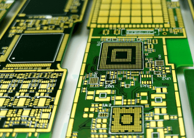
1. Increased Routing Density
By moving via connections internally, Buried Via PCB frees up outer layer space for:
-
Fine pitch components
-
High speed signal routing
-
Dense BGA breakout
This is especially important in modern compact electronics.
2. Improved Signal Integrity
Buried Via PCB reduces:
-
Via stubs
-
Signal reflection
-
Parasitic capacitance
This helps maintain stable impedance and supports high speed digital circuits.
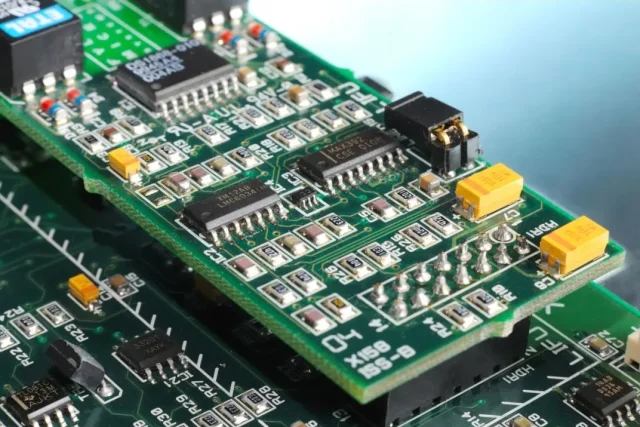
3. Compact and Space Efficient Design
Buried vias allow:
-
Smaller PCB size
-
Higher layer utilization
-
Efficient multilayer stack-up design
This is essential for smartphones, telecom boards, and server systems.
4. Enhanced Mechanical Reliability
Because buried vias are enclosed within the PCB:
-
They are protected from external stress
-
Reduced risk of solder-related issues
-
Improved structural stability
Applications of Buried Via PCB
Buried Via PCB is widely used in:
-
HDI PCB designs
-
Server and data center motherboards
-
Telecom infrastructure boards
-
5G communication equipment
-
Aerospace and defense electronics
-
High speed computing systems
These applications require high density routing, tight impedance control, and compact layout optimization.
Buried Via PCB vs Through-Hole PCB
| Feature | Buried Via PCB | Through-Hole PCB |
|---|---|---|
| Via Location | Internal Layers Only | Top to Bottom |
| Routing Density | High | Moderate |
| Signal Integrity | Improved | Standard |
| Manufacturing Complexity | High | Lower |
| Application | HDI & High Speed | General Electronics |
Buried Via PCB is preferred for advanced and high performance electronic systems.
Manufacturing Considerations
Producing Buried Via PCB requires:
-
Sequential lamination process
-
Precise inner layer alignment
-
Controlled drilling and plating
-
Strict quality inspection
-
Electrical testing of internal layers
An experienced PCB manufacturer ensures stable yield and high reliability for buried via structures.
Conclusion
Buried Via PCB enables high density routing, improved signal integrity, and compact multilayer PCB design.
By utilizing internal layer interconnections, Buried Via PCB supports advanced HDI structures and high speed digital systems while maintaining reliability and structural stability.
For telecom, server, aerospace, and high performance computing applications, Buried Via PCB is a key technology for modern PCB engineering.
