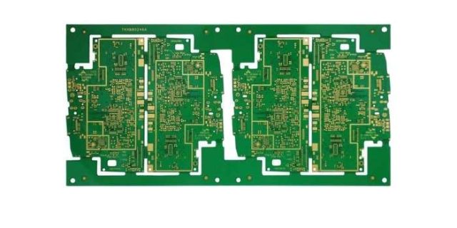
A Blind Via PCB is a multilayer printed circuit board that uses vias connecting an outer layer to one or more inner layers without extending through the entire board. Unlike through-hole vias, blind vias do not penetrate all layers, allowing for high-density routing, reduced board size, and improved signal integrity.
Blind via technology is critical in:
-
High-density consumer electronics
-
Smartphones, tablets, and laptops
-
High-speed networking and communication devices
-
Aerospace and defense systems
By enabling more efficient routing in multilayer boards, blind vias help designers maximize usable area while minimizing signal interference and crosstalk.
Design Advantages
Blind vias offer several significant advantages:
-
Space Efficiency:
They free up routing space on inner layers, allowing for higher component density and smaller PCB footprints. -
Improved Signal Integrity:
Shorter interconnect paths reduce parasitic capacitance and inductance, improving high-speed signal performance. -
Multilayer Routing Flexibility:
Designers can selectively connect specific layers, simplifying complex multilayer stack-ups. -
Reduced Crosstalk:
By limiting via penetration to only necessary layers, blind vias minimize interference between unrelated signal paths.
Engineering Challenges
Despite their advantages, blind vias present several engineering challenges:
-
Manufacturing Precision:
Drilling depth must be controlled within tight tolerances to avoid breaking through unwanted layers. -
Copper Plating Reliability:
Ensuring consistent plating within the blind via is critical for electrical connectivity and long-term reliability. -
Thermal Stress:
Blind vias can concentrate thermal stress during assembly or operation, requiring careful design and material selection. -
Cost Considerations:
Blind vias are more expensive than through-hole vias due to additional drilling and plating complexity. -
Via-in-Pad Design:
When blind vias are located directly under component pads, special attention is needed to prevent solder wicking and ensure robust solder joints.
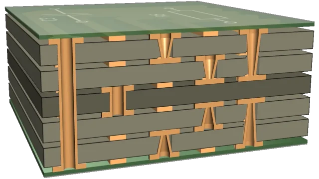
Fabrication Techniques
Producing blind via PCBs involves advanced manufacturing processes:
-
Laser or Mechanical Drilling:
Laser drilling is commonly used for microvias, providing precise depth control, while mechanical drilling is applied for larger blind vias. -
Electroplating:
Vias are plated with copper to ensure electrical connectivity and reliability. -
Stack-Up Lamination:
Careful lamination aligns multiple layers, preventing misregistration and voids in blind vias. -
Surface Finishes:
ENIG, immersion silver, or hard-gold finishes are applied to maintain solderability and signal performance. -
Quality Assurance:
-
X-ray inspection ensures via depth and plating quality
-
Electrical testing verifies continuity
-
Thermal cycling tests assess long-term reliability
-
KKPCB applies these advanced fabrication and QA techniques to produce blind via PCBs capable of supporting high-density, high-speed, and high-reliability applications.
Applications
Blind via PCBs are essential in applications that require high layer count, compact design, and precise signal routing:
-
Consumer Electronics: Smartphones, tablets, wearables with high-density PCBs
-
High-Speed Networking: Routers, switches, and server motherboards
-
Aerospace & Defense Electronics: Avionics and radar systems with tight space constraints
-
Medical Devices: Compact diagnostic and monitoring equipment
-
RF and Microwave Modules: High-frequency circuits requiring precise impedance control
By combining advanced via technology, precise layer stack-ups, and rigorous QA, KKPCB ensures blind via PCBs deliver reliable, high-performance solutions for modern high-density electronics.
