
With the increasing demand for compact, lightweight, and highly reliable electronic products, flexible printed circuit boards (Flex PCBs) have become an important solution for modern electronic design.
Compared with traditional rigid PCBs, Flex PCBs provide:
- Space-saving three-dimensional installation
- Reduced weight and thickness
- Improved mechanical flexibility
- Fewer connectors and wiring components
- Better resistance to vibration and mechanical stress
Among various flexible circuit structures, the 4-layer Flex PCB is widely used because it provides a good balance between:
- Routing density
- Electrical performance
- Mechanical flexibility
- Manufacturing feasibility
A well-designed 4-layer Flex PCB requires careful consideration of:
- Stackup structure
- Material selection
- Bend requirements
- Signal integrity
- Manufacturing process capability
This article explains the typical 4-layer Flex PCB stackup structure, manufacturing process, and key design guidelines.
1. What Is a 4 Layer Flex PCB?
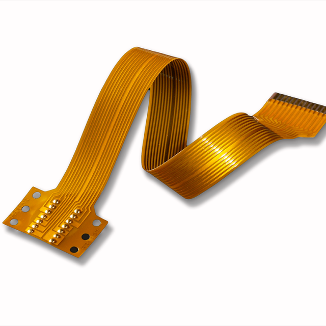
A 4-layer Flex PCB is a flexible circuit board consisting of four conductive copper layers connected through plated vias.
Compared with single-layer and double-layer Flex PCBs, a 4-layer structure provides:
- Higher wiring density
- Better power distribution
- Improved shielding capability
- More complex circuit routing
A typical 4-layer Flex PCB structure includes:
- Top copper layer
- First flexible dielectric layer
- Inner copper layer
- Core dielectric layer
- Inner copper layer
- Second flexible dielectric layer
- Bottom copper layer
The actual structure may vary depending on:
- Electrical requirements
- Mechanical bending conditions
- Manufacturing capability
2. Typical 4 Layer Flex PCB Stackup Structure
2.1 Standard 4 Layer Flex PCB Stackup
A common stackup configuration:
| Layer | Function |
|---|---|
| Layer 1 | Signal routing / component connection |
| Layer 2 | Signal, power, or ground layer |
| Layer 3 | Signal, power, or ground layer |
| Layer 4 | Signal routing / external connection |
Between copper layers, flexible dielectric materials provide:
- Electrical insulation
- Mechanical flexibility
- Structural support
3. Common Materials Used in 4 Layer Flex PCB Manufacturing
3.1 Polyimide (PI) Material
Polyimide is the most widely used flexible PCB material.
Advantages:
- Excellent flexibility
- High temperature resistance
- Good dimensional stability
- Strong chemical resistance
Applications:
- Medical devices
- Automotive electronics
- Wearable electronics
3.2 Adhesive-Free Flex Materials
Adhesive-free materials are increasingly used in advanced Flex PCB applications.
Advantages:
- Reduced thickness
- Better dimensional stability
- Improved electrical performance
Suitable for:
- High-density Flex PCBs
- Fine-pitch applications
3.3 Coverlay Materials
Coverlay replaces traditional solder masks in flexible circuits.
Functions:
- Protect copper traces
- Improve mechanical durability
- Provide electrical insulation
3.4 Stiffener Materials
Stiffeners are added to specific areas where mechanical support is required.
Common stiffener materials:
- FR-4
- Polyimide
- Stainless steel
Applications:
- Connector areas
- Component mounting regions
4. Key Considerations for 4 Layer Flex PCB Stackup Design
4.1 Balance Between Flexibility and Layer Count
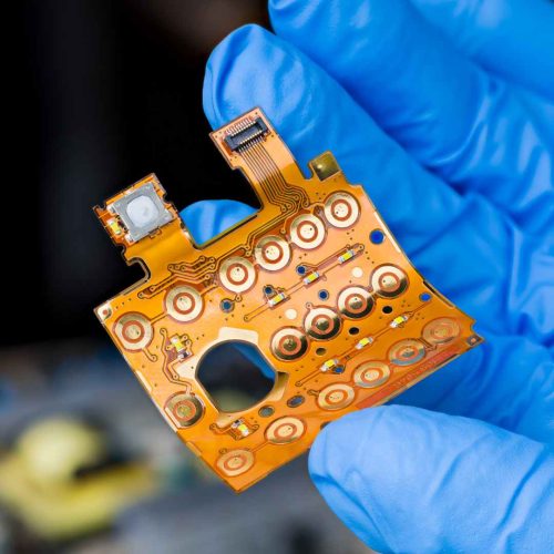
Increasing the number of layers improves routing capability but reduces flexibility.
A 4-layer Flex PCB must balance:
- Copper thickness
- Dielectric thickness
- Total board thickness
A thicker structure may provide better durability but reduce bending performance.
4.2 Copper Layer Arrangement
Copper distribution significantly affects mechanical reliability.
Recommended practices:
- Maintain balanced copper distribution
- Avoid large copper differences between layers
- Reduce stress concentration areas
Uneven copper distribution may cause:
- Board deformation
- Mechanical stress
- Bending reliability problems
4.3 Signal Layer Planning
For high-speed applications, stackup planning should consider:
- Signal reference planes
- Return current paths
- Impedance control
A common arrangement is:
- Outer layers for signal routing
- Inner layers for power and ground reference
This helps improve:
- EMI performance
- Signal integrity
4.4 Impedance Control in 4 Layer Flex PCBs
For applications such as:
- RF modules
- High-speed communication
- Sensor systems
controlled impedance is critical.
Factors affecting impedance include:
- Copper thickness
- Trace width
- Dielectric thickness
- Material dielectric constant
Manufacturers may use:
- Stackup simulation
- TDR testing
to verify impedance requirements.
5. 4 Layer Flex PCB Manufacturing Process
5.1 Engineering Review and DFM Analysis
Before production, engineers review:
- Gerber files
- Stackup requirements
- Bend areas
- Manufacturing limitations
DFM analysis helps identify:
- Minimum trace limitations
- Via risks
- Assembly challenges
5.2 Material Preparation
The manufacturing process begins with:
- Flexible laminate preparation
- Coverlay preparation
- Stiffener preparation
Material selection depends on:
- Electrical requirements
- Mechanical requirements
- Operating environment
5.3 Circuit Pattern Formation
The circuit pattern is created through:
- Photo imaging
- Etching
- Copper processing
Precision control is required for:
- Fine traces
- Layer alignment
- Circuit accuracy
5.4 Drilling and Via Formation
4-layer Flex PCBs typically require:
- Through vias
- Microvias
- Laser drilling
Important parameters include:
- Hole diameter
- Registration accuracy
- Copper plating reliability
5.5 Layer Lamination
Multiple flexible layers are laminated together under controlled conditions.
Key parameters:
- Temperature
- Pressure
- Lamination time
Poor lamination may result in:
- Delamination
- Layer shifting
- Reduced reliability
5.6 Surface Finishing
Common surface finishes include:
ENIG
Advantages:
- Flat surface
- Good solderability
- Suitable for fine-pitch components
ENEPIG
Advantages:
- Higher reliability
- Suitable for advanced applications
OSP
Advantages:
- Cost-effective
- Suitable for specific assembly requirements
6. Manufacturing Challenges of 4 Layer Flex PCBs
6.1 Layer Alignment Accuracy
Multiple flexible layers require precise registration.
Alignment errors may cause:
- Via connection failures
- Circuit performance issues
6.2 Via Reliability
Flexible circuits experience mechanical stress.
Poor via design may cause:
- Copper cracking
- Intermittent electrical failures
6.3 Bending Reliability
Repeated bending can affect:
- Copper conductors
- Adhesive layers
- Coverlay structures
Design must consider:
- Static bending
- Dynamic bending cycles
6.4 Thermal Expansion Control
Different materials have different expansion characteristics.
Poor material matching may cause:
- Layer separation
- Dimensional instability
7. Design Guidelines for 4 Layer Flex PCB
7.1 Avoid Routing in Dynamic Bend Areas
High-stress areas should avoid:
- Vias
- Solder joints
- Large copper areas
7.2 Use Rounded Trace Corners
Sharp corners increase mechanical stress.
Recommended:
- Curved routing
- Smooth trace transitions
7.3 Control Bend Radius
The minimum bend radius depends on:
- Material thickness
- Copper thickness
- Number of layers
Proper bend radius improves:
- Mechanical life
- Electrical reliability
7.4 Consider Assembly Requirements
For Flex PCBA applications, consider:
- SMT support tooling
- Stiffener requirements
- Component placement limitations
8. Applications of 4 Layer Flex PCBs
8.1 Medical Electronics
Applications:
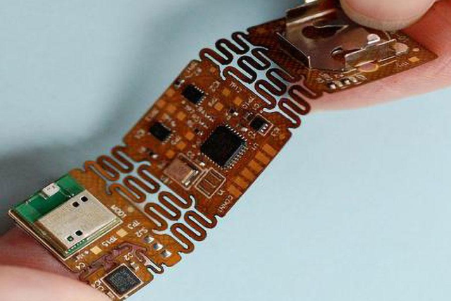
- Wearable monitoring devices
- Diagnostic equipment
- Portable medical systems
Requirements:
- Compact structure
- High reliability
8.2 Automotive Electronics
Applications:
- Sensor modules
- Control systems
- Interior electronics
Requirements:
- Vibration resistance
- Temperature stability
8.3 Consumer Electronics
Applications:
- Smartphones
- Cameras
- Smart wearable devices
Requirements:
- Thin design
- Space optimization
8.4 Industrial Equipment
Applications:
- Control modules
- Embedded systems
- Measurement equipment
Requirements:
- Long-term reliability
- Mechanical durability
9. Future Development Trends of 4 Layer Flex PCB Technology
Future Flex PCB development will focus on:
Higher Density Integration
Driven by:
- Miniaturized electronics
- Advanced packaging
Better High-Speed Performance
Driven by:
- 5G communication
- IoT devices
- High-frequency applications
Improved Reliability
Through:
Conclusion
A 4-layer Flex PCB provides an effective solution for electronic products requiring high wiring density, compact structure, and mechanical flexibility.
Successful manufacturing requires careful optimization of:
- Stackup design
- Material selection
- Copper distribution
- Impedance control
- Bend reliability
- Manufacturing process capability
By applying proper design guidelines and advanced manufacturing technologies, 4-layer Flex PCBs can achieve reliable performance in demanding applications including medical devices, automotive electronics, communication systems, and industrial equipment.
