The Growing Importance of Multilayer PCB Technology
As modern electronic products continue evolving toward:
- higher performance
- smaller size
- faster data transmission
- greater functionality
- intelligent automation
traditional single-layer and double-sided PCBs can no longer meet the demands of advanced electronic systems.
Today, multilayer PCB technology has become essential in industries such as:
- telecommunications
- industrial automation
- automotive electronics
- aerospace systems
- medical devices
- AI computing
- 5G communication
- consumer electronics
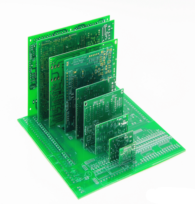
A multilayer PCB allows engineers to integrate:
- complex signal routing
- high-speed digital circuits
- RF transmission lines
- power distribution networks
- grounding structures
within a compact PCB structure.
Compared with standard PCB structures, multilayer PCB design provides:
- higher circuit density
- improved signal integrity
- stronger EMI suppression
- enhanced power distribution
- better thermal performance
This article explains:
- the multilayer PCB manufacturing process
- multilayer PCB advantages
- multilayer PCB applications
- fabrication technologies
- stack-up design considerations
- future trends in multilayer PCB engineering
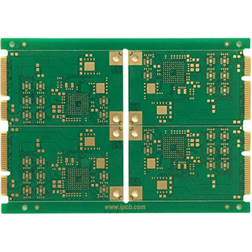
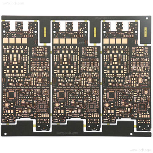
What Is a Multilayer PCB?
Definition of Multilayer PCB
A multilayer PCB is a printed circuit board composed of:
- three or more conductive copper layers
laminated together using: - prepreg materials
- insulating substrates
These conductive layers are interconnected through:
- plated through holes (PTH)
- blind vias
- buried vias
- microvias
Multilayer PCBs are designed to support:
- complex circuit routing
- high-density interconnections
- controlled impedance structures
- advanced power management
Typical Multilayer PCB Structures
Common multilayer PCB configurations include:
- 4-layer PCB
- 6-layer PCB
- 8-layer PCB
- 10-layer PCB
- 12-layer PCB
- HDI multilayer PCB
Advanced systems may exceed:
- 20-layer PCB structures
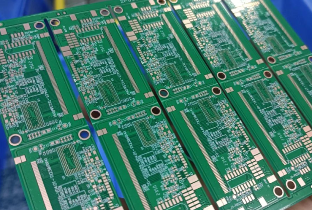
Multilayer PCB Manufacturing Process
1. PCB Design and Engineering Preparation
The manufacturing process begins with:
- PCB layout design
- stack-up planning
- impedance calculation
- DFM analysis
Critical design considerations include:
- signal integrity
- power integrity
- thermal management
- EMI control
- layer arrangement
Design software generates:
- Gerber files
- drill files
- fabrication drawings
2. Inner Layer Core Preparation
The internal copper-clad laminates are prepared for:
- inner circuit imaging
The process includes:
- material cutting
- surface cleaning
- oxide treatment
High-quality preparation improves:
- copper adhesion
- multilayer bonding reliability
3. Inner Layer Imaging
Photoresist is applied onto:
- inner copper layers
UV exposure transfers:
- PCB circuit patterns
onto: - the photoresist layer
This process defines:
- signal traces
- power planes
- ground structures
4. Inner Layer Etching
Unwanted copper is chemically removed to form:
- PCB circuit patterns
Etching precision directly affects:
- trace width accuracy
- impedance consistency
- signal integrity
Fine-line etching is especially critical for:
- HDI PCB
- RF PCB
- high-speed PCB systems
5. Automated Optical Inspection (AOI)
AOI systems inspect:
- inner layer defects
- open circuits
- short circuits
- trace geometry accuracy
This ensures:
- multilayer PCB quality
- manufacturing reliability
6. Layer Alignment and Lamination
The etched inner layers are stacked together with:
- prepreg insulation layers
- copper foil
The multilayer stack is laminated under:
- high temperature
- high pressure
Lamination forms:
- a unified multilayer PCB structure
Critical parameters:
- temperature control
- pressure balance
- resin flow management
7. Drilling Process
Mechanical drilling or laser drilling creates:
- via holes
- mounting holes
- blind vias
- buried vias
High-precision drilling is essential for:
- multilayer interconnection reliability
- HDI PCB fabrication
8. Hole Metallization and Copper Plating
The drilled holes are chemically treated and plated with copper.
This creates electrical connections between:
- multilayer PCB layers
Copper plating quality affects:
- signal reliability
- current carrying capability
- long-term durability
9. Outer Layer Imaging and Etching
Outer layers undergo:
- photo imaging
- copper etching
This creates:
- final PCB circuitry
- RF transmission lines
- high-speed routing structures
10. Solder Mask Application
Solder mask protects the PCB from:
- oxidation
- solder bridging
- environmental contamination
Common solder mask colors:
- green
- black
- blue
- red
11. Surface Finish Process
Surface finishes improve:
- solderability
- corrosion resistance
- assembly reliability
Common PCB surface finishes:
- ENIG
- HASL
- immersion silver
- immersion tin
12. Silkscreen Printing
Silkscreen printing adds:
- component labels
- logos
- assembly markings
13. Electrical Testing
Electrical testing verifies:
- open circuits
- short circuits
- connectivity accuracy
Testing methods include:
- flying probe testing
- bed-of-nails testing
14. Final Inspection and Quality Control
Final inspection checks:
- dimensional accuracy
- layer alignment
- surface quality
- impedance performance
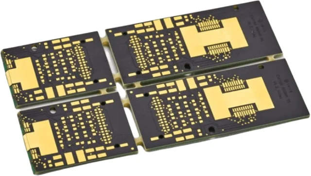
Advantages of Multilayer PCB
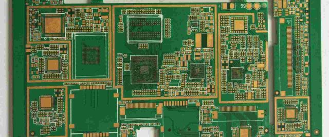
1. High Circuit Density
Multilayer PCB design supports:
- complex routing
- compact layouts
- high component density
This is essential for:
- smartphones
- servers
- networking hardware
- RF modules
2. Improved Signal Integrity
Dedicated ground and power planes improve:
- impedance control
- signal return paths
- noise suppression
Benefits:
- reduced signal reflection
- lower crosstalk
- better high-speed performance
3. Enhanced EMI Suppression
Multilayer PCB structures provide:
- electromagnetic shielding
- stable grounding
- improved EMC performance
Widely used in:
- RF PCB
- automotive electronics
- aerospace systems
4. Better Power Distribution
Power planes improve:
- voltage stability
- current distribution
- power integrity
Critical for:
- AI servers
- industrial control systems
- high-current electronics
5. Compact Product Design
Multilayer PCB technology enables:
- smaller product size
- higher integration
- lightweight electronics
6. Improved Thermal Management
Copper planes assist:
- heat spreading
- thermal dissipation
- temperature control
Applications:
- power electronics PCB
- motor driver PCB
- LED PCB
7. Greater Mechanical Reliability
Multilayer structures provide:
- stronger PC
- B rigidity
- vibration resistance
- durability
Applications of Multilayer PCB
Multilayer PCB technology is widely used in:
1. Telecommunications
- 5G base stations
- networking equipment
- RF communication modules
2. Automotive Electronics
- automotive radar
- EV control systems
- ADAS modules
3. Aerospace and Defense
- satellite systems
- military communication
- avionics electronics
4. Industrial Automation
- PLC controllers
- robotics systems
- industrial motor control
5. Medical Devices
- imaging equipment
- patient monitoring systems
- portable medical electronics
6. Consumer Electronics
- smartphones
- laptops
- gaming systems
- wearable devices
7. AI and Data Centers
- GPU servers
- AI accelerators
- high-speed networking hardware
Challenges in Multilayer PCB Manufacturing
1. Complex Fabrication Process
Multilayer PCB manufacturing requires:
- advanced equipment
- tight process control
- skilled engineering
2. Higher Manufacturing Cost
Additional layers increase:
- material usage
- processing complexity
- inspection requirements
3. Thermal Stress Management
Large multilayer structures may experience:
- warpage
- delamination
- thermal expansion mismatch
4. Impedance Control Challenges
High-speed PCB systems require:
- precise dielectric thickness
- accurate trace geometry
- stable stack-up design
Future Trends in Multilayer PCB Technology
1. HDI Multilayer PCB Development
Supporting:
- ultra-fine routing
- microvias
- compact electronics
2. High-Speed PCB Materials
Enabling:
- 112G/224G networking
- AI computing
- advanced RF communication
3. Embedded Component PCB Technology
Including:
- embedded capacitors
- embedded resistors
- integrated cooling structures
4. AI-Driven PCB Manufacturing
Using:
- automated optical analysis
- predictive quality control
- intelligent process optimization
Conclusion
Multilayer PCB technology has become one of the most important foundations of modern electronics manufacturing.
- multilayer PCB fabrication
- stack-up engineering
- impedance control
- thermal management
- EMI suppression
manufacturers can achieve:
- compact electronic systems
- high-speed signal performance
- reliable power distribution
- excellent long-term durability
The advantages of multilayer PCB include:
- higher circuit density
- improved signal integrity
- enhanced thermal performance
- stronger EMI control
- compact product integration
As electronic systems continue evolving toward:
- higher speed
- greater functionality
- increased miniaturization
- advanced RF integration
multilayer PCB technology will remain essential for the future of:
-
- telecommunications
- AI computing
- aerospace electronics
- industrial automation
- automotive systems
