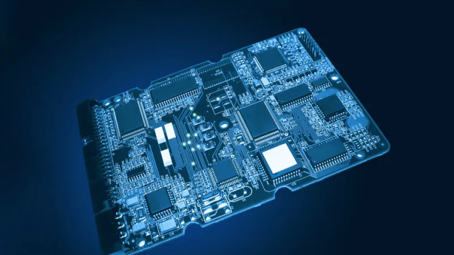
Advanced PCBs represent the cutting edge of printed circuit board technology, enabling compact, high-performance, and highly reliable electronic systems for demanding applications such as 5G/6G infrastructure, ADAS automotive radar, AI computing, aerospace electronics, Industrial IoT, and medical devices. These boards go far beyond standard FR-4 designs, incorporating HDI (High-Density Interconnect), rigid-flex, high-frequency low-loss materials, heavy copper, and complex multilayer stack-ups to deliver superior signal integrity, thermal management, power handling, and miniaturization.
At KKPCB, we specialize in advanced PCB solutions with full turnkey capabilities — from expert design support and precision manufacturing to high-reliability PCBA (Printed Circuit Board Assembly). Our state-of-the-art processes ensure first-pass success, tight tolerances, and compliance with stringent standards including IPC-6012 Class 3, IATF 16949, and AEC-Q100 for automotive and industrial-grade applications.
Key Types of Advanced PCBs
Modern electronics require specialized PCB technologies to meet performance and form-factor demands:
- HDI PCBs: Feature microvias, blind/buried vias, and fine-line/spacing (down to 2 mil/0.05 mm) for higher component density and shorter signal paths. Ideal for smartphones, wearables, and high-speed computing.
- High-Frequency / RF / Microwave PCBs: Built with low-loss laminates such as Rogers RO3003, RO4835, Panasonic Megtron 6/7, and Isola IS680 to minimize insertion loss and maintain stable dielectric constant (Dk) at GHz frequencies — critical for 77 GHz radar, 5G backhaul, and E-Band links.
- Rigid-Flex and Flex PCBs: Combine rigid sections for component mounting with flexible polyimide layers for dynamic bending. Perfect for space-constrained or vibration-heavy environments like aerospace, defense, and portable medical devices.
- Heavy Copper PCBs: Support high current applications in EV power systems, industrial controls, and power electronics with copper weights of 2 oz to 20 oz+.
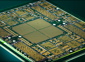
- Multilayer PCBs (up to 80+ layers): Provide complex routing, dedicated power/ground planes, and excellent EMI shielding for high-speed digital designs (DDR5/6, PCIe 6.0/7.0, 112G-PAM4).
Advanced PCB Design Best Practices
Successful advanced PCB projects begin with intelligent design that balances performance, manufacturability, and cost:
- Stack-Up Optimization: Symmetric designs with balanced copper distribution to minimize warpage. Use dedicated ground planes adjacent to high-speed signals for controlled impedance (50 Ω / 100 Ω ±5%).
- Signal Integrity & High-Speed Routing: Short traces, differential pairs, via shielding, back-drilling, and EM simulation to reduce reflections, crosstalk, and jitter.
- Thermal Management: Thermal vias, copper pours, metal-core options, and careful component placement to dissipate heat from high-power ICs and MMICs.
- Power Integrity: Low-impedance PDN with strategic decoupling and split planes where needed.
- DFM (Design for Manufacturability): Early collaboration with the manufacturer to validate trace widths, via aspect ratios, annular rings, clearances, and panelization.
- DFA & DFT: Optimize for SMT assembly (fine-pitch components, stencil design) and testability (test points, boundary scan).
KKPCB’s engineering team provides professional PCB layout services supporting up to 64+ layers, 110,000+ pins, and high-speed interfaces, with free DFM feedback on every project.
Advanced PCB Manufacturing Process
Producing advanced PCBs demands precision equipment and tightly controlled processes:
- Material Preparation & DFM Review — Selection of high-Tg, low-loss, or flexible substrates with vacuum-sealed storage.
- Inner Layer Imaging & Etching — Laser direct imaging (LDI) for fine features and automated optical inspection (AOI).
- Precision Drilling — Mechanical and laser drilling for microvias, blind/buried vias, with advanced desmear and plasma treatment.
- Multilayer Lamination — Vacuum-assisted presses with optimized temperature and pressure profiles for uniform thickness and reliable registration.
- Plating & Outer Layer Processing — High-reliability copper plating, fine-line etching, and surface finishes such as ENIG or ENEPIG for excellent solderability and low RF loss.
- Solder Mask, Silkscreen & Profiling — Durable masks and precise routing for complex rigid-flex or HDI boards.
- Electrical Testing & Inspection — 100% E-test, TDR/VNA impedance verification, X-ray, and cross-section analysis.
KKPCB supports HDI, rigid-flex, heavy copper, and hybrid constructions with exceptional layer-to-layer alignment and yield.
Advanced PCB Assembly (PCBA) Capabilities
Advanced PCBA transforms bare boards into functional assemblies with high yield and reliability:
- SMT, DIP, and Hybrid Assembly — Supporting fine-pitch BGAs, QFNs, 0201/01005 components, and mixed-technology builds on 14+ SMT lines.
- Component Sourcing — Global procurement with strict quality verification and counterfeit prevention.
- Advanced Processes — Selective soldering, conformal coating, underfill, potting, and press-fit for rugged applications.
- Testing & Quality Assurance — AOI, X-ray (for BGA voids), ICT, functional testing, burn-in, and RF calibration for high-frequency modules.
- Box-Build & System Integration — Full enclosure assembly, cable harnesses, and final product testing.
Our processes minimize defects like tombstoning, bridging, and voids while ensuring compliance with automotive and industrial reliability standards.
KKPCB’s Advantages in Advanced PCBs
- Comprehensive Capabilities: HDI, rigid-flex, high-frequency, heavy copper, multilayer, and hybrid PCBs up to 80+ layers.
- Material Expertise: Rogers, Megtron, Isola, and flexible substrates with tight Dk/Df control.
- One-Stop Turnkey Service: Design, fabrication, component sourcing, PCBA, testing, and global delivery from prototype to high-volume production.
- Quality Certifications: IPC Class 3, IATF 16949, ISO standards, and support for AEC-Q100 automotive requirements.
- Fast Turnaround & Reliability: Rapid prototypes, seamless scaling, and proven performance in 5G, ADAS, AI, and industrial applications.
Future Trends in Advanced PCBs
In 2026 and beyond, advanced PCBs are evolving toward greater integration with AI-driven design tools, finer HDI features, embedded components, 2.5D/3D packaging, sustainable materials, and higher thermal/electrical performance to support software-defined vehicles, edge AI, and 6G networks. KKPCB continues investing in automation, precision processes, and next-generation materials to stay ahead of these trends.
Ready to bring your advanced electronics project to life with superior advanced PCBs? Share your Gerber files, stack-up requirements, schematic, or application details with the KKPCB team. Receive free expert DFM analysis, material recommendations, impedance modeling, thermal simulations, fast-turn prototypes, and competitive volume quotes.
Partner with KKPCB for reliable, high-performance advanced PCB design, manufacturing, and assembly that accelerates your time-to-market and ensures long-term product success.
