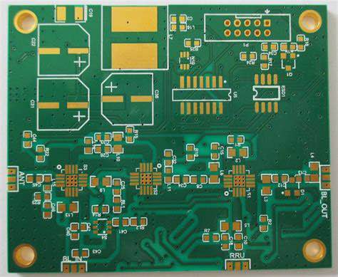
In the fast-growing world of Industrial IoT (IIoT) and Wireless Sensor Networks (WSN), reliable wireless communication is essential for real-time monitoring, predictive maintenance, and smart factory operations. Megtron 6, Panasonic’s high-performance low-loss PCB material, is widely chosen for these applications because of its excellent dielectric properties: stable Dk (dielectric constant) around 3.2–3.6 and ultra-low Df (dissipation factor) of ~0.002 at high frequencies. However, even minor variations in dielectric consistency can degrade signal integrity, increase insertion loss, and shorten communication range—issues that directly impact battery life, data accuracy, and system uptime in harsh industrial environments.
At KKPCB, we specialize in optimizing Megtron 6 PCBs to deliver superior dielectric uniformity and RF efficiency, helping IIoT and WSN manufacturers achieve longer transmission distances, lower power consumption, and rock-solid performance in vibration, temperature swings, and EMI-heavy settings.
Why Dielectric Consistency and RF Efficiency Matter for IIoT and WSN
- Dielectric Consistency refers to the uniformity of Dk, Df, and board thickness across a panel, batch, and even within individual layers. Inconsistent dielectric properties cause impedance mismatch, phase jitter, and unpredictable antenna behavior—critical problems for 2.4 GHz, 5 GHz, Sub-GHz, and emerging 5G/6G IIoT modules.
- RF Efficiency is measured by low insertion loss, minimal return loss, and high gain in antennas and RF traces. Every 0.1 dB improvement in loss can extend sensor battery life by 5–10 % or increase reliable range by several meters in industrial plants.
Without tight control, even premium Megtron 6 can suffer from resin-content variation, copper-foil roughness, or lamination-induced stress, leading to yield loss and field failures.
Key Challenges in Megtron 6 PCB Fabrication
Megtron 6’s low-resin, high-glass-content structure makes it sensitive to:
- Resin flow and thickness variation during lamination
- Surface roughness of copper foil (standard RTF vs. VLP/HVLP)
- Moisture absorption during storage and processing
- Stack-up asymmetry and copper distribution imbalance
- Etching tolerances that affect trace geometry at RF frequencies
These factors can cause ±0.05 Dk variation or 5–10 % impedance deviation—unacceptable for precision wireless sensor nodes.
Proven Techniques to Improve Dielectric Consistency and RF Efficiency
KKPCB applies a combination of advanced process controls, material engineering, and verification methods specifically tailored for Megtron 6:
- Precision Material Handling & Storage Megtron 6 is stored in climate-controlled rooms (≤ 25 °C / 50 % RH) with vacuum-sealed packaging and strict FIFO protocols to eliminate moisture-induced Dk drift.
- Optimized Lamination Process
- Symmetric stack-ups with balanced copper weights and identical prepreg types on both sides
- Tight control of lamination pressure, temperature ramp, and dwell time using vacuum-assisted presses
- Real-time resin-flow monitoring to achieve thickness tolerance of ±5 µm across large panels
- Advanced Copper Foil Selection Use of very-low-profile (VLP) or hyper-very-low-profile (HVLP) copper foils reduces conductor loss by up to 30 % at 5–10 GHz while maintaining excellent adhesion.
- Controlled Impedance Design & Fabrication
- 3D field solvers during DFM to predict and compensate for Dk variation
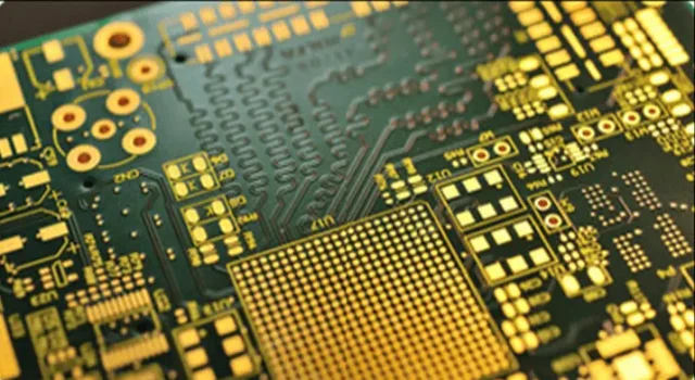
- Laser direct imaging (LDI) and fine-line etching for trace width/spacing tolerances ≤ 10 µm
- Post-etch annealing and surface treatment to stabilize dielectric properties
- Rigorous Testing & Verification
- Cavity resonator or split-post dielectric resonator (SPDR) method for Dk/Df mapping across the panel
- Time-Domain Reflectometry (TDR) and Vector Network Analyzer (VNA) measurements up to 20 GHz
- Thermal cycling and reflow simulation to confirm stability under industrial operating conditions (-40 °C to +125 °C)
- Full-panel dielectric scanning to guarantee < ±0.02 Dk variation (industry-leading for Megtron 6)
- Surface Finish Optimization ENIG or ENEPIG with ultra-thin nickel layers minimizes skin-effect loss while providing excellent solderability for RF components and antennas.
KKPCB’s Advantages for Megtron 6 IIoT and WSN PCBs
- Material Expertise — Certified Panasonic partner with extensive experience in Megtron 6, Megtron 7, and other high-frequency laminates (Rogers, Taconic, Isola).
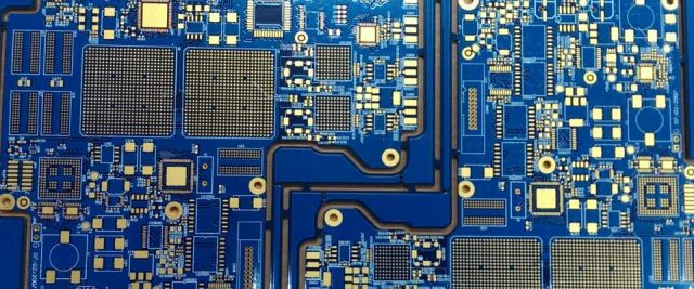
- High-Frequency Capabilities — Up to 80-layer boards, HDI, embedded antennas, and hybrid stack-ups (Megtron 6 + FR-4 for cost optimization).
- One-Stop Turnkey Service — From DFM and material sourcing to full PCBA with RF calibration, functional testing, and enclosure integration.
- Quality Certifications — IPC-6012 Class 3, ISO 9001, IATF 16949, and customer-specific RF performance reports.
- Proven Results — Our optimized Megtron 6 boards routinely achieve < 0.15 dB/inch insertion loss at 10 GHz and impedance tolerance of ±5 %, delivering 15–25 % better RF range and efficiency compared to standard processes.
Real-World Benefits for Industrial IoT and Wireless Sensor Networks
Optimized Megtron 6 PCBs from KKPCB enable:
- Longer battery life in remote sensors and edge nodes
- Higher data throughput in dense factory mesh networks
- Robust performance in high-vibration, high-temperature, and EMI environments
- Faster time-to-market through reduced tuning iterations and higher first-pass yield
Whether you are designing vibration-resistant machine-health monitors, smart-grid wireless gateways, or autonomous robot communication modules, consistent dielectric performance translates directly into lower total cost of ownership and higher system reliability.
Ready to Elevate Your IIoT and WSN Designs?
At KKPCB we turn Megtron 6’s outstanding material properties into repeatable, production-ready RF performance. Send us your Gerber files, stack-up requirements, or target frequency bands. Our RF engineering team will provide:
- Free DFM analysis with dielectric consistency and loss-budget predictions
- Competitive quotation with fast prototype turnaround (5–7 days standard)
- Full electrical and thermal verification reports
Contact KKPCB today and experience the difference that true dielectric consistency and RF efficiency can make in your industrial wireless projects.
