1. Introduction: Why Multilayer PCBs Are Essential in Modern Electronics
As electronic devices continue to evolve toward miniaturization, high-speed performance, and multifunction integration, traditional single-layer or double-layer PCBs can no longer meet design requirements.
This has led to the widespread adoption of multilayer PCBs (Multilayer Printed Circuit Boards), which integrate multiple conductive layers within a single compact structure.
Multilayer PCBs are now the backbone of:
- High-speed computing systems
- RF and microwave communication modules
- Automotive electronics (ECU, ADAS)
- Industrial control systems
- Medical and aerospace electronics
At KKPCB, multilayer PCB production is optimized for high reliability, controlled impedance, and advanced HDI integration.
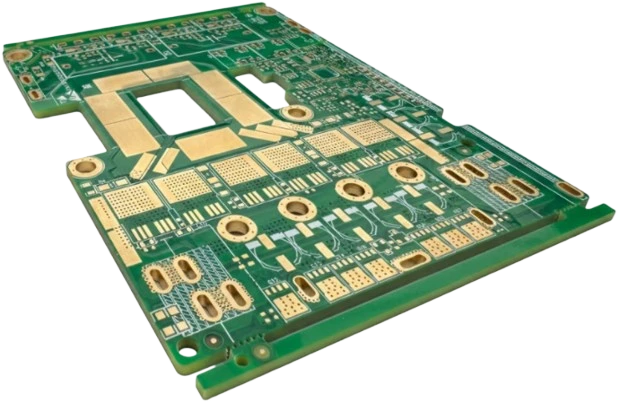
2. What Is a Multilayer PCB?
A multilayer PCB consists of three or more conductive copper layers stacked together with insulating dielectric materials.
Typical structure includes:
- Top signal layer
- Internal signal/power layers
- Ground layers
- Bottom signal layer
These layers are bonded together using high-pressure lamination technology, forming a compact and high-performance circuit board.
3. Multilayer PCB Manufacturing Process
The manufacturing of multilayer PCBs involves multiple precision-controlled steps:
3.1 Inner Layer Circuit Patterning
- Copper-clad laminates are cleaned and coated with photoresist
- Circuit patterns are exposed using UV lithography
- Unwanted copper is etched away
- Inner layers are inspected (AOI testing)
This step defines the core electrical routing structure.
3.2 Layer Alignment and Lamination
Inner layers are stacked with:
- Prepreg (PP resin sheets)
- Copper foils
Then subjected to:
- High temperature
- High pressure
This process bonds all layers into a single solid structure.
Proper lamination ensures:
- Mechanical strength
- Electrical stability
- Controlled dielectric spacing
3.3 Drilling (Mechanical & Laser Drilling)
After lamination:
- Through-holes are drilled for inter-layer connectivity
- Laser drilling is used for microvias in HDI PCBs
Precision drilling is critical for:
- Signal integrity
- Via reliability
- High-density routing
3.4 Copper Plating (Electroless + Electroplating)
- Holes are cleaned and activated
- Thin copper layer is deposited (electroless plating)
- Electroplating thickens copper to required conductivity
This ensures:
- Strong electrical interconnection
- Reliable via conductivity
3.5 Outer Layer Patterning
Similar to inner layers:
- Photo imaging process
- Etching of unwanted copper
- Formation of final circuit patterns
3.6 Solder Mask and Surface Finish
Protective layers are applied:
- Solder mask for insulation
- Surface finish (ENIG, HASL, OSP, etc.)
This improves:
- Solderability
- Oxidation resistance
- Long-term reliability
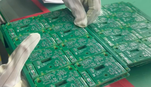
3.7 Electrical Testing and Inspection
Final PCB testing includes:
- Continuity testing
- Short-circuit detection
- Impedance verification
- AOI inspection
- X-ray inspection for multilayer alignment
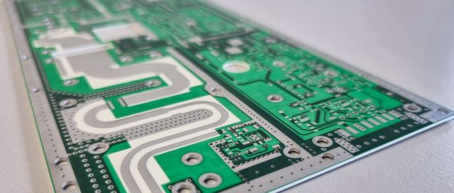
4. Advantages of Multilayer PCBs
4.1 High-Density Circuit Integration (HDI Capability)
Multilayer PCBs allow:
- Complex routing in limited space
- Reduced board size
- High component density
This is essential for smartphones, IoT devices, and compact electronics.
4.2 Improved Signal Integrity
With proper stack-up design:
- Reduced EMI
- Controlled impedance routing
- Stable high-speed signal transmission
This is critical in RF, microwave, and high-speed digital systems.
4.3 Better Power Distribution
Dedicated power and ground planes provide:
- Stable voltage distribution
- Reduced noise coupling
- Improved system stability
4.4 Enhanced Thermal Management
Multilayer structures help:
- Spread heat evenly
- Reduce thermal hotspots
- Improve system reliability
4.5 High Reliability and Durability
Compared to single-layer boards:
- Stronger mechanical structure
- Better vibration resistance
- Higher long-term stability
5. Applications of Multilayer PCBs
Multilayer PCBs are widely used in:
5.1 Consumer Electronics
- Smartphones
- Laptops
- Wearable devices
5.2 Automotive Electronics
- Engine control units (ECU)
- ADAS radar systems
- Infotainment systems
5.3 Communication Systems
- 5G/6G base stations
- RF modules
- Network routers
5.4 Industrial Equipment
- Automation controllers
- Power systems
- Robotics
5.5 Aerospace & Medical
- Flight control systems
- Satellite communication
- Medical imaging devices
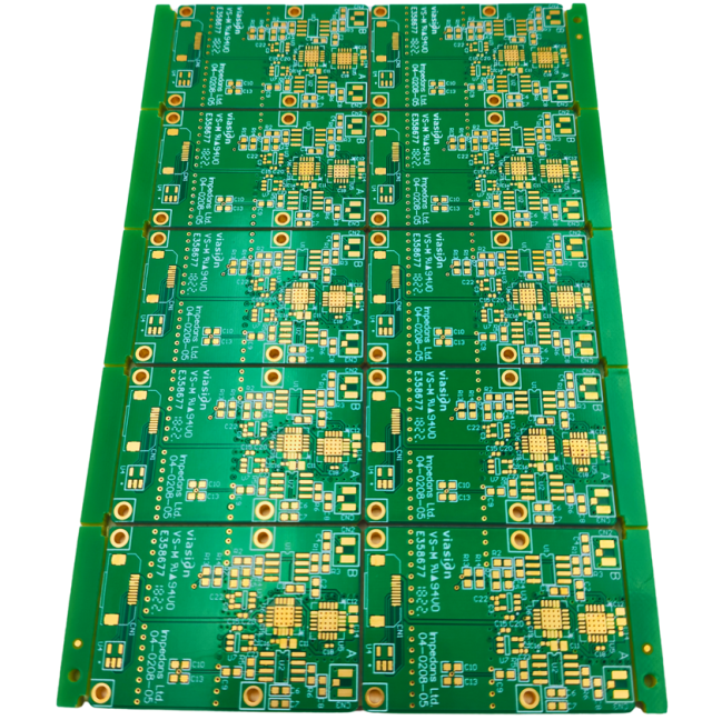
6. KKPCB Multilayer PCB Manufacturing Capabilities
At KKPCB, multilayer PCB production includes:
- Up to high layer-count stack-up design
- Controlled impedance manufacturing (±5%)
- HDI microvia technology
- Advanced lamination process control
- Strict DFM & DFA engineering review
Quality assurance includes:
- AOI inspection
- X-ray layer alignment
- Electrical testing
- Thermal reliability testing
This ensures stable performance in high-frequency, high-speed, and harsh environment applications.
7. Conclusion
Multilayer PCB technology is the foundation of modern electronic system design, enabling high-density integration, improved signal integrity, better power distribution, and superior reliability.
As electronic systems become more complex and high-speed, multilayer PCB manufacturing will continue to play a critical role in next-generation technology development.
With advanced engineering and precision manufacturing capability, KKPCB delivers high-performance multilayer PCB solutions for automotive, communication, industrial, and aerospace industries.
