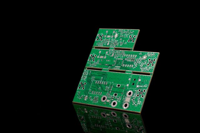
In modern PCB design, Blind Via and Buried Via technologies play a critical role in achieving high-density interconnect (HDI) structures, improving signal integrity, and optimizing PCB layout performance. As electronic devices continue to evolve toward miniaturization, high speed, and high functionality, the use of blind vias and buried vias has become increasingly essential in advanced multilayer PCB manufacturing.
A blind via is a type of via that connects the outer layer of a PCB to one or more inner layers without passing through the entire board. This structure helps designers maximize usable routing space on inner layers, making blind vias ideal for HDI PCB designs, smartphones, servers, and high-speed communication devices. By using blind via technology, engineers can significantly enhance signal routing efficiency and reduce electromagnetic interference (EMI).
On the other hand, a buried via connects only inner layers of a multilayer PCB and is not visible from the outer surface. Buried vias are widely used in complex PCB stack-ups, allowing for improved signal integrity, reduced signal loss, and better impedance control. Since buried vias do not occupy space on outer layers, they enable higher component density and more compact PCB layouts.
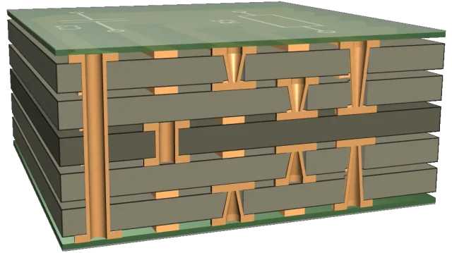
Both blind vias and buried vias are essential technologies in HDI PCB fabrication, but they require advanced manufacturing processes, such as laser drilling, sequential lamination, and precise registration control. Compared to traditional through-hole vias, blind and buried vias increase PCB fabrication cost, but they offer significant advantages in performance, reliability, and space optimization.
When choosing between blind via and buried via structures, designers must consider factors such as PCB layer count, signal speed, thermal management, and cost constraints. For high-frequency PCBs and high-speed digital circuits, using blind vias and buried vias can greatly reduce signal reflection, improve power integrity, and enhance overall electrical performance.
In conclusion, Blind Via and Buried Via technologies are indispensable for modern PCB manufacturing, especially in applications requiring high density, high performance, and compact design. By leveraging these advanced via structures, manufacturers and engineers can achieve superior PCB reliability, optimized signal transmission, and next-generation electronic product performance.
