
Megtron 6 PCB projects often fail late for a simple reason: the electrical loss budget was written before the stackup, copper profile, and connector geometry were frozen. A material family can support demanding high-speed channels, but the released board still depends on resin content, finished dielectric thickness, reference-plane continuity, copper roughness, and fabrication capability. This guide gives engineers and project managers a practical way to turn a channel target into a buildable multilayer release.
Table of Contents
- Channel loss budget
- Stackup and copper controls
- Launch and transition review
- Verification and release checklist
For a material overview, review the Megtron 6 PCB capability page with the stackup owner before the loss budget is frozen.
Start with the channel budget, not the material name
When the program uses a Megtron 6 PCB for a dense serial link, the loss budget should be signed off with the stackup owner.
At the architecture stage, divide the end-to-end loss into package escape, connector launch, vias, copper, dielectric, and any cable or filter contribution. The laminate is only one term. Panasonic MEGTRON 6 family data shows that typical Dk and Df values depend on the exact construction and test method; a single family label is not a substitute for a controlled stackup. Use the selected grade and glass style as a starting point, then ask the fabricator to model the finished dielectric thickness rather than the nominal core catalogue value.
For a server, switch, radar, or converter channel, the useful engineering question is not “Which laminate is fastest?” It is “Which construction keeps insertion loss, impedance, skew, and registration inside the same release window?” That wording prevents a late material substitution from invalidating the equalization plan.
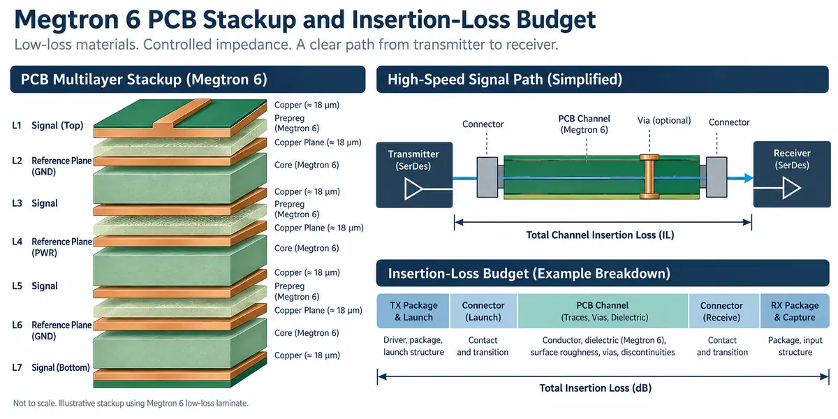
The Megtron 6 PCB build must be checked against actual press, copper, and drill windows.
Translate datasheet values into a stackup that can be built
Control dielectric thickness and glass style
Two laminates with similar nominal Dk can produce different impedance when resin content, weave, and pressed thickness change. Build the stackup around the signal pair, its adjacent planes, and the finished copper. Define the impedance target, acceptable tolerance, and the test coupon geometry together. If a 100-ohm differential pair is routed beside a plane opening or across a weave transition, the local field can move even when the average calculation looks correct.
Budget conductor loss realistically
At multi-gigabit edge rates, copper roughness and plating shape matter as much as line width. Request the intended copper foil type, finished copper range, and etch compensation in the fabrication notes. A wide trace that is over-etched can lose the intended impedance; a plated microvia that is underfilled can create a discontinuity at the launch. KKPCB’s high-speed PCB manufacturing review should therefore include both the electrical target and the process window that protects it.
Keep the return path continuous
Route every fast transition against a solid reference plane. When a pair changes layers, place the return vias close to the signal vias and keep anti-pad changes symmetrical. Avoid long neck-downs under connectors, split planes beneath the pair, and stitching patterns that force return current around a void. The Megtron 6 materials page is useful for confirming the selected family, but the released impedance still belongs to the complete construction.
In a production review, the Megtron 6 PCB layer map is the common language between signal-integrity and CAM teams.
Design the launch and transition before routing the channel
The most robust Megtron 6 PCB launch is reviewed with the connector vendor, layout engineer, and fabricator together.
Many “laminate” failures are actually launch failures. A press-fit connector, edge connector, or coax transition creates a short three-dimensional region where pad diameter, antipad, back-drill depth, solder mask, and ground-via spacing interact. Review that region in 2D and in a cross-section view before the rest of the channel is routed. Keep the pair reference plane uninterrupted through the launch and remove unused via stubs when the frequency range makes them resonant.
For a mixed-signal module, the PCB layout review should compare the electrical model with the actual layer map. A change from one press construction to another can move a pair toward a plane or change the via barrel length. Record the layer, reference plane, target impedance, and transition type in the release table so that design, CAM, and fabrication use the same definition.
The second diagram shows a conceptual differential route, connector launch, and via transition. It is a design aid, not a measured customer result.
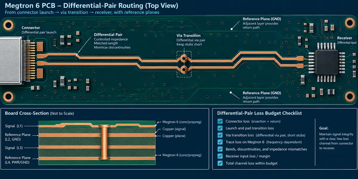
A final Megtron 6 PCB handoff also records the assembly constraints that protect the launch.
Verification and manufacturing handoff
A Megtron 6 PCB release is easier to defend when electrical, mechanical, and fabrication assumptions are written in one package.
Before release, compare field-solver output, coupon geometry, and fabrication notes. Specify which impedance method is used, where the coupon sits in the panel, and how the result will be correlated to the product layer. Ask for a cross-section plan that can verify dielectric thickness, copper distribution, plated-hole quality, and registration around dense breakouts. The same evidence package supports PCB assembly planning because connector coplanarity, solder-mask clearance, and reflow exposure can change the launch after fabrication.
For a prototype program, freeze the material grade, stackup revision, surface finish, and coupon definition before ordering. Use PCB prototype assembly to expose connector and thermal issues early, but do not treat a prototype coupon as a universal guarantee for a later panel design. If the design is moved to volume, recheck the panel array, copper balance, and drill strategy rather than assuming the prototype process transfers unchanged.
For a project manager, this Megtron 6 PCB record makes supplier comparison and revision control auditable.
Release checklist for the project team
- Named material grade, glass style, finished dielectric targets, and test method.
- Loss budget separated into dielectric, conductor, connector, via, and package terms.
- Pair impedance, skew, copper range, and etch-compensation limits defined.
- Launch, back-drill, return-via, and reference-plane rules shown on the layer drawing.
- Coupon location, cross-section request, and acceptance window included in the purchase package.
- Any material or stackup substitution routed through engineering change control.
Sources: Panasonic Industrial Devices MEGTRON 6 family and R-5775/R-5670 technical data; supporting high-speed interconnect guidance from Analog Devices and Qorvo application material; KKPCB pages for manufacturing, layout, assembly, prototype assembly, and MEGTRON 6 material capability. Values in this article are typical or design-reference values unless a released drawing defines the acceptance limit.
